Semiconductor Device and Manufacturing Method Thereof

a semiconductor device and semiconductor technology, applied in the direction of semiconductor devices, electrical devices, transistors, etc., can solve the problems of difficult to obtain high yield, complex structure, and need for transistor formation, so as to reduce the parasitic capacitance or junction capacitance of the transistor, reduce the power consumption of the semiconductor device, and reduce the relative permittivity

Inactive Publication Date: 2008-10-30
SEMICON ENERGY LAB CO LTD
View PDF18 Cites 33 Cited by
  • Summary
  • Abstract
  • Description
  • Claims
  • Application Information

AI Technical Summary

Benefits of technology

[0012]In a transistor included in a semiconductor device of the present invention, a semiconductor film and a cavity are in contact with each other. Thus, parasitic capacitance or junction capacitance of the transistor can be reduced when the cavity is filled with air, nitrogen, an inert gas, or the like that has lower relative permittivity than an inorganic insulating film of silicon oxide or the like. Thus, reduction in po...

Problems solved by technology

However, as for the transistor having the SON structure described in Patent Document 1, a great amount of hydrogen gas, which requires careful handling in a manufacturing process, is used, and furthermore the transistor is needed to be formed through a complicated process due to difficulty in control of the thickness of the semi...

Method used


Image

  • Semiconductor Device and Manufacturing Method Thereof
  • Semiconductor Device and Manufacturing Method Thereof
  • Semiconductor Device and Manufacturing Method Thereof

Examples


embodiment mode 1

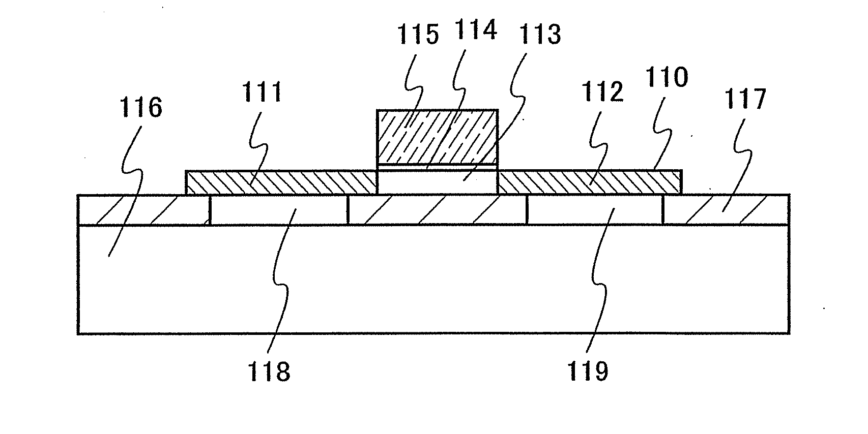
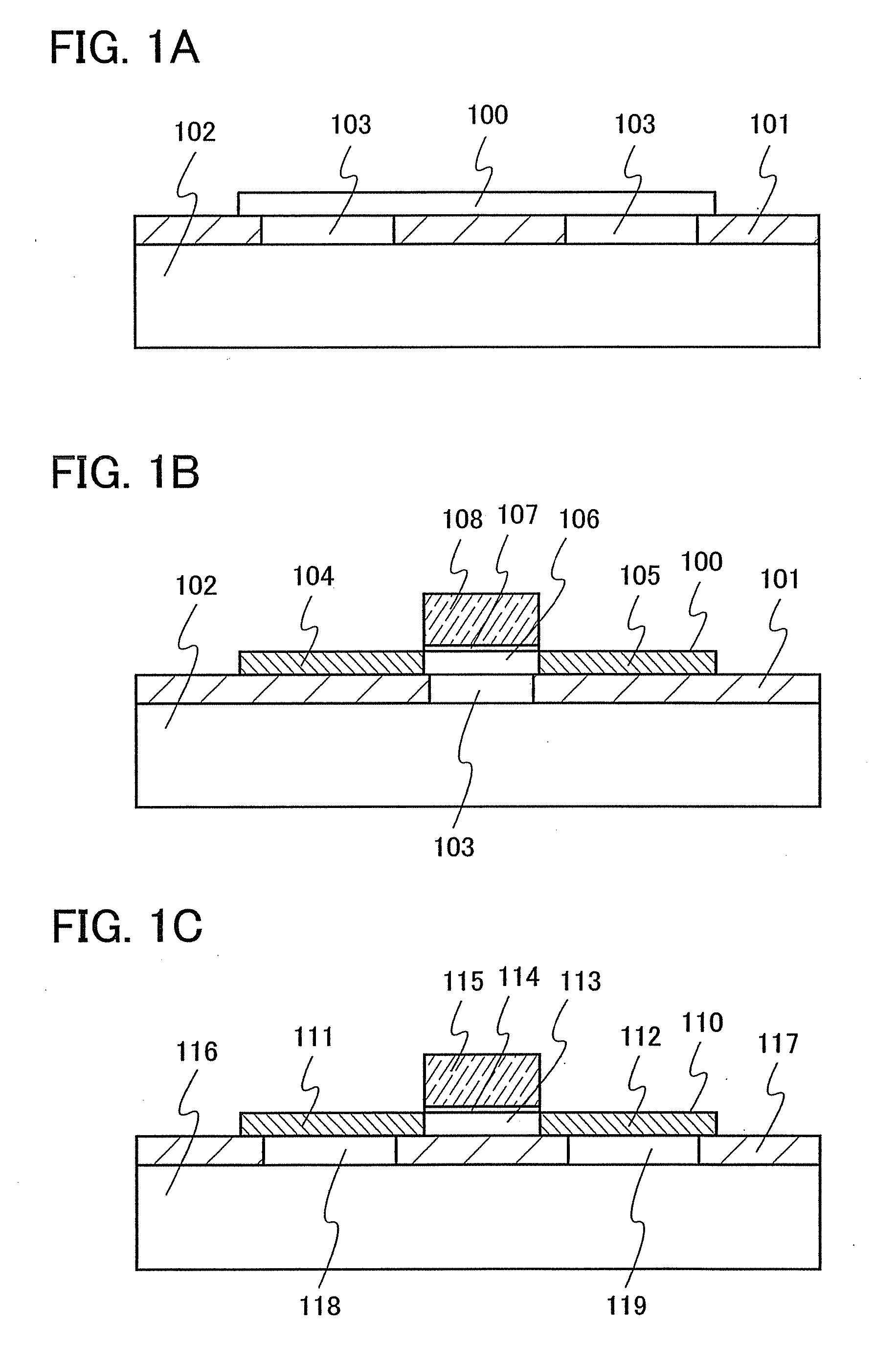
[0036]A structure of a semiconductor film included in a semiconductor element in a semiconductor device of the present invention will be described with reference to FIG. 1A.

[0037]A semiconductor film 100 shown in FIG. 1A is formed over a base substrate 102 so that an insulating film 101 is interposed therebetween. The insulating film 101 and the semiconductor film 100 are bonded to each other, whereby the semiconductor film 100 can be bonded to the base substrate 102. The insulating film 101 includes at least one opening, which forms a cavity 103 between the semiconductor film 100 and the base substrate 102. A part of the cavity 103 or the whole cavity 103 overlaps with a part of the semiconductor film 100, and thus at least a part of the insulating film 101 overlaps with the semiconductor film 100 at a region of the insulating film 101 other than the opening. The number of cavities 103 is not limited to the structure shown in FIG. 1A. One cavity 103 or a plurality of cavities 103 m...

embodiment mode 2

[0047]In this embodiment mode, a structure of a transistor included in a semiconductor device of the present invention will be described more specifically.

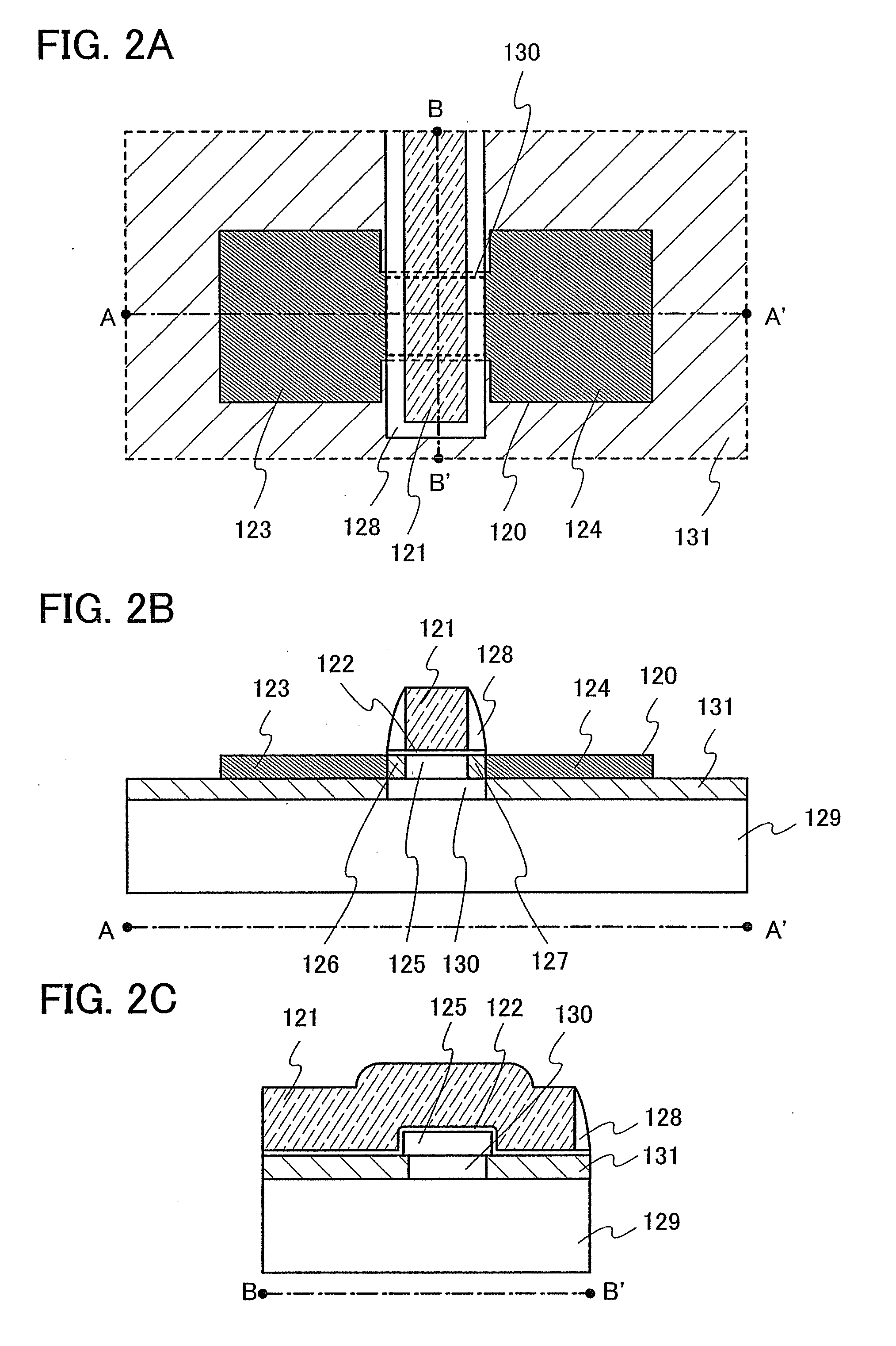
[0048]FIG. 2A shows an example of a top view of a transistor included in a semiconductor device of the present invention and FIGS. 2B and 2C each show an example of a cross-sectional view thereof. FIG. 2A is a top view of the transistor, FIG. 2B is a cross-sectional view taken along line A-A′ in FIG. 2A, and FIG. 2C is a cross-sectional view taken along line B-B′ in FIG. 2A.

[0049]The transistor shown in FIGS. 2A to 2C includes a semiconductor film 120 functioning as an active layer, an electrode 121, a portion of which overlapping with the semiconductor film 120 functions as a gate, and a gate insulating film 122 provided between the semiconductor film 120 and the electrode 121. The semiconductor film 120 includes impurity regions 123 and 124, one of which functions as a source and the other as a drain, a channel formation region ...

embodiment mode 3

[0074]In this embodiment mode, a manufacturing method of a semiconductor device of the present invention, in which a semiconductor film is transferred from a semiconductor substrate (a bond substrate) to a supporting substrate (a base substrate) over which an insulating film including an opening is formed will be described.

[0075]First, as shown in FIG. 6A, hydrogen or a noble gas, or hydrogen ions or noble gas ions is introduced into the bond substrate 200 as indicated by arrows, whereby a defect layer 201 having very small voids is formed in a region at a certain depth from a surface of the bond substrate 200. The position where the defect layer 201 is formed is determined depending on acceleration voltage at the time of the above-described introduction. The thickness of a semiconductor film 205 which is transferred from the bond substrate 200 to a base substrate is determined by the position of the defect layer 201; therefore, acceleration of the voltage at the time of the introdu...


PUM


Abstract

An object is to provide a semiconductor device in which, through a simpler process, junction capacitance and power consumption can be reduced more than a conventional semiconductor device, and a manufacturing method thereof. An insulating film including an opening is formed over a base substrate and a part of a bond substrate is transferred to the base substrate, with the insulating film interposed therebetween, whereby a semiconductor film including a cavity between the semiconductor film and the base substrate is formed over the base substrate. Then, a semiconductor device including a semiconductor element such as a transistor is manufactured using the semiconductor film. The transistor includes a cavity between the base substrate and the semiconductor film used as an active layer. One cavity may be provided or a plurality of cavities may be provided.

Description

BACKGROUND OF THE INVENTION[0001]1. Field of the Invention[0002]The present invention relates to a semiconductor device using an SOI (silicon on insulator) substrate and a manufacturing method of the semiconductor device. In particular, the present invention relates to a bonding SOI technique, a semiconductor device using an SOI substrate which is obtained in such a manner that a single crystal semiconductor film or a polycrystalline semiconductor film is bonded to a substrate with an insulating film interposed therebetween, and a manufacturing method of the semiconductor device.[0003]2. Description of the Related Art[0004]Demands for higher integration, higher operation speed, higher performance, and lower power consumption have been more stringent, and in response to the above-described demands, a transistor using an SOI substrate has attracted an attention as effective means that can take the place of a bulk transistor. Higher operation speed and lower power consumption can be ex...

Claims


Application Information

Patent Timeline
IPC IPC(8): H01L29/786H01L21/30
CPCH01L27/1214H01L27/1266H01L29/78621H01L29/66772H01L29/78603H01L29/66757H01L21/764H01L21/2007H01L21/18H01L27/12
Inventor MIYAIRI, HIDEKAZU
Owner SEMICON ENERGY LAB CO LTD
Why Eureka
Try Eureka