Microscale optoelectronic device packages

Active Publication Date: 2008-11-27
WOLFSPEED INC
View PDF38 Cites 145 Cited by
  • Summary
  • Abstract
  • Description
  • Claims
  • Application Information

AI Technical Summary

Benefits of technology

[0017]A further aspect of the invention relates to an optoelectronic device article comprising: a substrate containing at least one electrically conductive microvia; at least one emitter diode adapted to emit radiation and disposed in or on the substrate; at least one ESD diode disposed in or on the substrate; a first electrically conductive path between t

Problems solved by technology

Numerous applications for LEDs and laser diodes would benefit from greater flux density; however, various considerations thermal and packaging constraints have limited the ability flux density output of conventional optoelectronic devices.
Packaging and thermal constraints, however, currently limit the ability for multiple LEDs to operate at high flux densities while being disposed very close together.
LEDs, especially gallium nitride-based LEDs, are par

Method used


Image

  • Microscale optoelectronic device packages
  • Microscale optoelectronic device packages
  • Microscale optoelectronic device packages

Examples


first embodiment

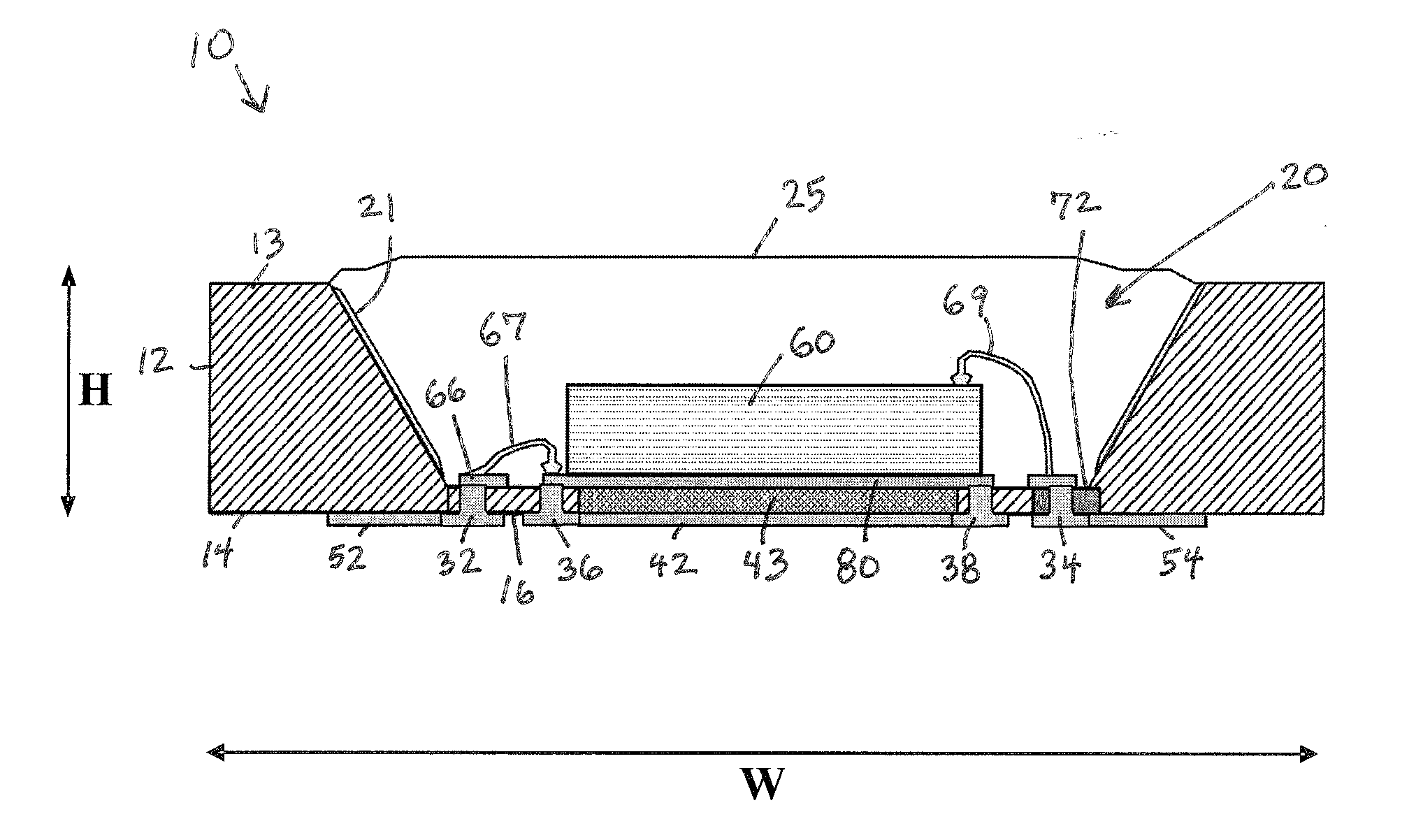
[0058]FIG. 1 is a cross-sectional schematic view of at least a portion of a microscale optoelectronic device package 10 according to the present invention, the package 10 including an emitter diode 60 disposed within a reflector cavity 20 bounded in part by a membrane portion 16 of a substrate 12. The membrane portion 16 defines a plurality of microvias 32, 34, 36, 38 and includes an ESD diode 72 disposed along the membrane portion 16. As illustrated, the microvias 32, 34, 36, 38 have substantially vertical sidewalls, such as may be formed with an anisotropic etch through the substrate 12; however, as indicated previously, such microvias may be formed of any convenient or desirable size or shape. The substrate 12 includes a front or upper surface 13 (along which radiation is transmitted outward from the emitter diode 60) and an opposing backside or lower surface 14. The reflector cavity 20 has a reflective material 21 (e.g., aluminum or other metal) deposited along the side walls th...

second embodiment

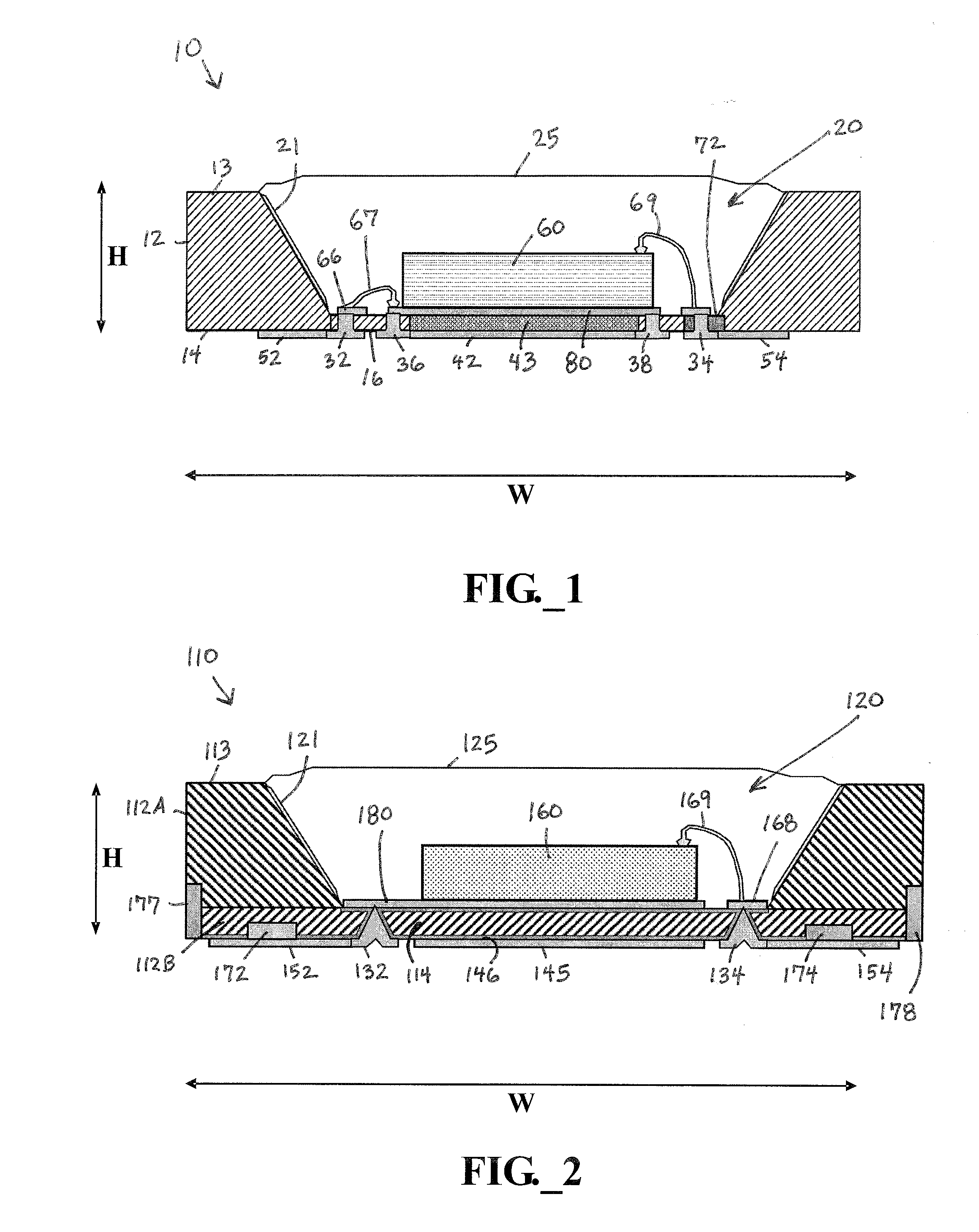
[0062]FIG. 2 is a cross-sectional schematic view of at least a portion of a microscale optoelectronic device package 110 the package 110 including ESD diodes 172, 174 disposed along a backside surface 114 of a substrate composed of substrate layers 112A, 112B, and an emitter diode 160 disposed within a reflector cavity 120 (having a deposited reflective material 121) bounded in part by a membrane portion 115 of the substrate. The membrane portion 115 defines a plurality of microvias 132, 134 disposed on either side of a thermal contact pad 145 beneath the emitter diode 160. Since the microvias 132, 134 are spatially separated from the thermal contact pad 145, the thermal contact pad 145 can be electrically isolated. In the case of a silicon substrate, electrical isolation is achieved by the formation or addition of an insulating surface layer 146 (e.g., silicon dioxide) that coats most or all of the substrate surface prior to the metallization of the microvias and contact pads. Sin...

third embodiment

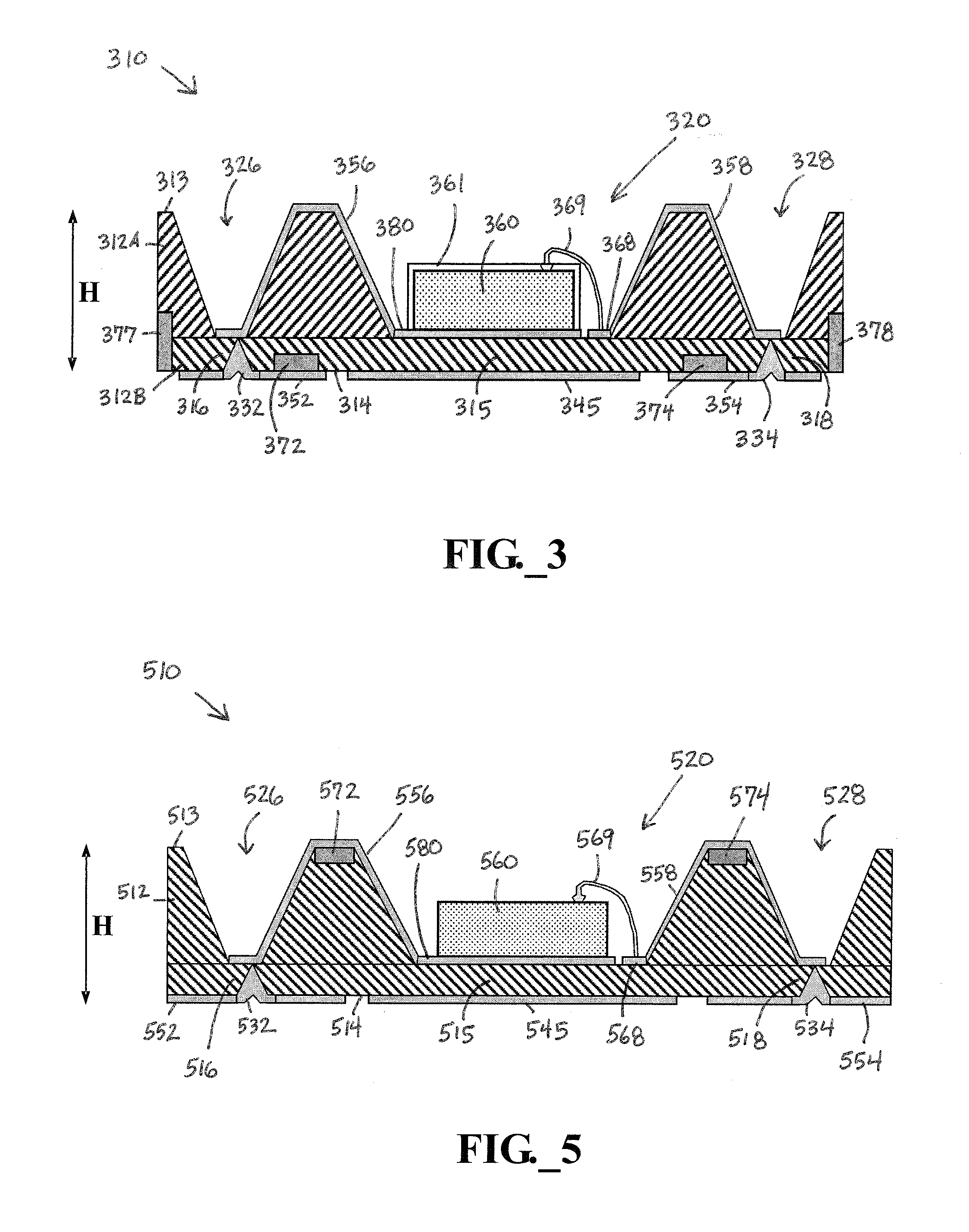
[0066]Referring to FIG. 3, such figure provides a cross-sectional schematic view of at least a portion of a microscale optoelectronic device package 310 the package 310 including ESD diodes 372, 374 disposed along a backside surface 314 of a substrate composed of substrate layers 312A, 312B. An emitter diode 360 having a phosphor layer 361 deposited thereon is disposed in a reflector cavity 320 bounded in part by a first membrane portion 315. The substrate further defines additional cavities 326, 328 that are non-adjacent to the emitter diode 360 and bounded by second membrane portions 316, 318 of the substrate that define microvias 332, 334 located remotely from the emitter diode 360. The upper substrate layer 312A is preferably formed of a readily etchable material, such as N-type silicon, whereas the lower substrate layer 312B is preferably formed of a less-etchable material, such as P-type silicon, to serve as an etch stop in formation of the cavities 320, 326, 328, such that t...


PUM


Abstract

An optoelectronic device article comprises a substrate containing at least one electrically conductive microvia, at least one emitter diode and at least one ESD diode, optionally formed in situ, disposed in or on the substrate, and an electrically conductive path between the foregoing elements. A reflector cavity may be defined in the substrate for receiving the emitter diode(s), with retention elements on the substrate used to retain a lens material. High flux density and high emitter diode spatial density may be attained. Thermal sensors, radiation sensors, and integral heat spreaders comprising one or more protruding fins may be integrated into the article.

Description

FIELD OF THE INVENTION[0001]The present invention relates to optoelectronic devices including light emitting diodes and / or laser diodes, and to systems employing the same.BACKGROUND OF THE INVENTION[0002]Optoelectronic devices such as light emitting diodes (LEDs) and laser diodes have numerous applications and are growing in popularity. LEDs—including those outputting white and other colors of light—are used, for example, for general and automotive illumination, for backlights in liquid crystal and other displays, for high color rendering index devices, and for color mixing devices. Laser diodes are used, for example, in various communication applications, including transmitters for optical fiber communications systems and single-mode pump diodes for fiber amplifiers. LEDs and laser diodes are solid state devices each having a P-N junction semiconductor diode that emits radiation (e.g., infrared radiation, visible radiation, ultraviolet radiation, and so on) responsive to applicatio...

Claims


Application Information

Patent Timeline
IPC IPC(8): H01L33/00H01L21/00H01L33/48
CPCH01L25/167H01L33/486H01S5/0206H01S5/06825H01L2224/48227H01L2224/48465H01L2924/00H01L2224/8592H01L2924/19107H01L2924/00012
Inventor MEDENDORP, JR., NICHOLAS W.IBBETSON, JAMES
Owner WOLFSPEED INC
Why Eureka
Try Eureka