Enhanced copper posts for wafer level chip scale packaging

a technology of scale packaging and copper posts, applied in the direction of electrical equipment, semiconductor devices, semiconductor/solid-state device details, etc., can solve the problems of preventing crack propagation, and achieve the effects of improving the shear strength of the entire wlcsp assembly, improving conductivity, and improving the resistance to crack propagation

Active Publication Date: 2008-12-04
ADVANCED MFG INNOVATIONS INC
View PDF4 Cites 60 Cited by
  • Summary
  • Abstract
  • Description
  • Claims
  • Application Information

AI Technical Summary

Benefits of technology

[0013]An advantage of a preferred embodiment of the present invention is that by forming the conducting pins that are eventually encapsulated within the solder balls, the shear strength of the entire WLCSP assembly is increased.
[0014]A further advantage of a preferred embodiment of the present invention is improved conductivity. The additional pin or pins create additional surface areas between the electrode the solder ball. Therefore, the electrical connection between the s

Problems solved by technology

Moreover, creating an irregularly shaped solder joint retards the propagation of crack

Method used


Image

  • Enhanced copper posts for wafer level chip scale packaging
  • Enhanced copper posts for wafer level chip scale packaging
  • Enhanced copper posts for wafer level chip scale packaging

Examples


Embodiment Construction

[0026]The making and using of the presently preferred embodiments are discussed in detail below. It should be appreciated, however, that the present invention provides many applicable inventive concepts that can be embodied in a wide variety of specific contexts. The specific embodiments discussed are merely illustrative of specific ways to make and use the invention, and do not limit the scope of the invention.

[0027]The present invention will be described with respect to preferred embodiments in a specific context, namely a copper post WLCSP. The invention may also be applied, however, to other materials used in providing the conductive connections between the packaging and the wafer or die.

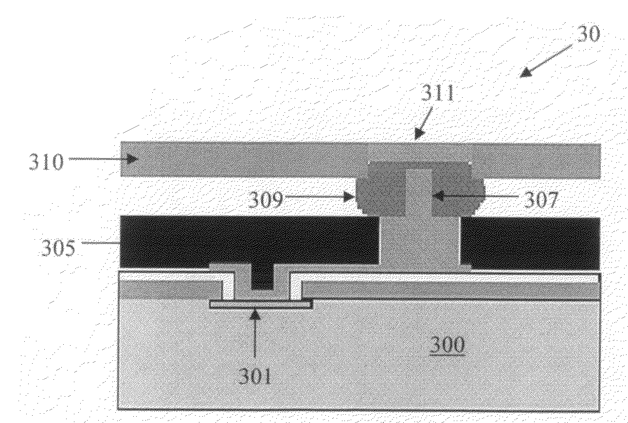
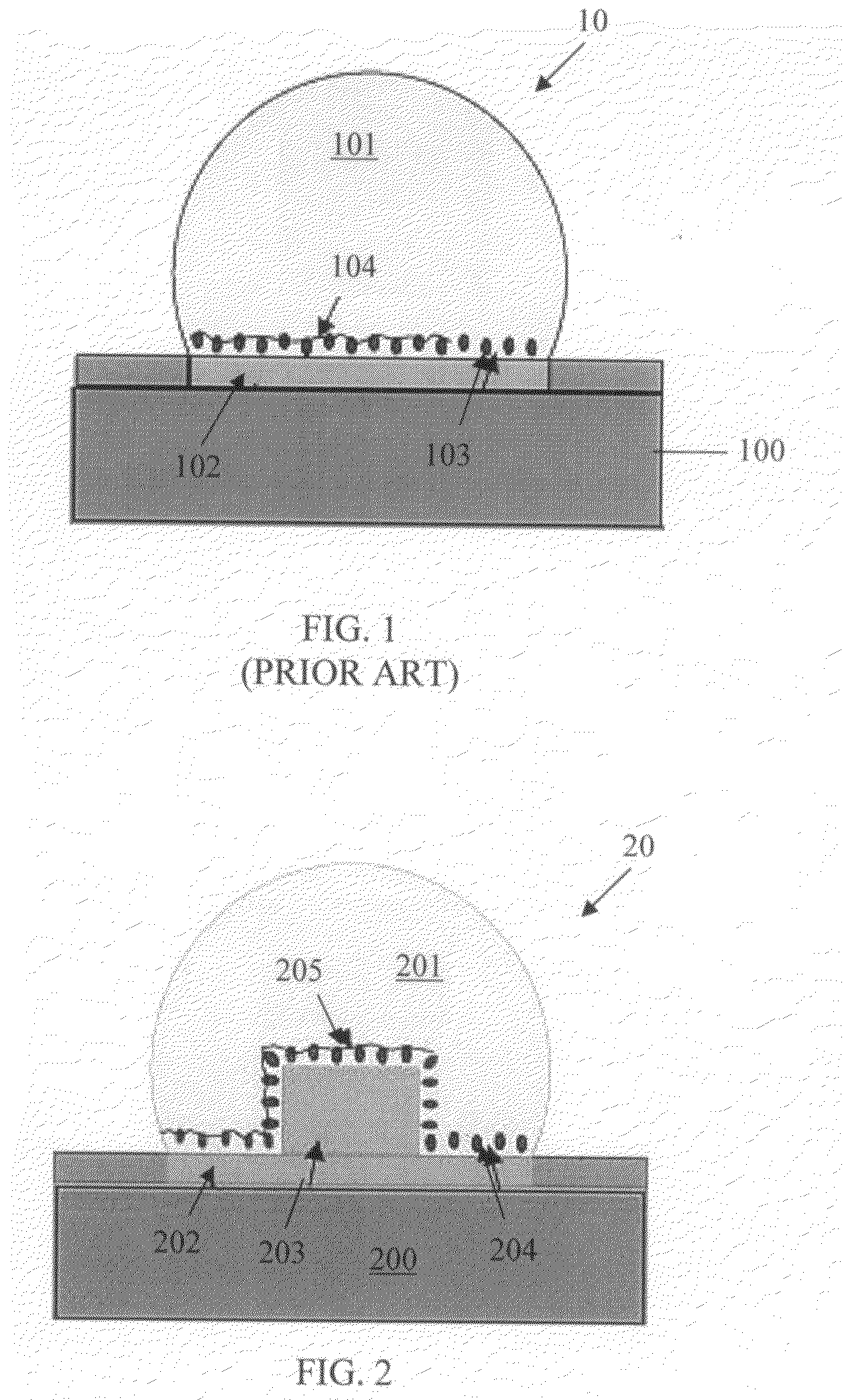
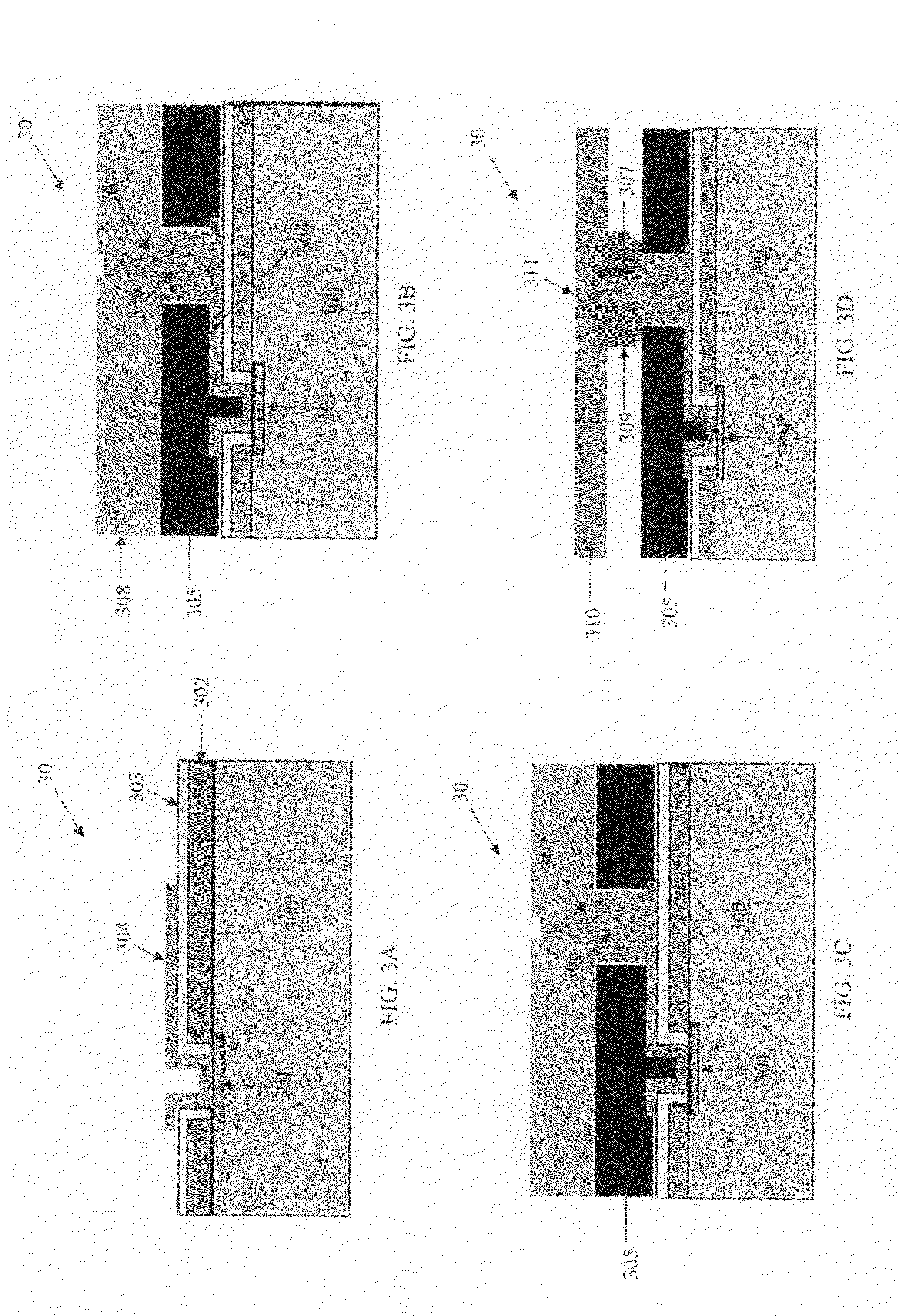
[0028]With reference now to FIG. 2, there is shown a cross-sectional view of WLCSP feature 20 configured according to one embodiment of the present invention. Conducting pad 202 is formed into die 200 as a base for the contact and bonding mechanism for solder ball 201. In addition to conducting ...


PUM


Abstract

An enhanced wafer level chip scale packaging (WLCSP) copper electrode post is described having one or more pins that protrude from the top of the electrode post. When the solder ball is soldered onto the post, the pins are encapsulated within the solder material. The pins not only add shear strength to the soldered joint between the solder ball and the electrode post but also create a more reliable electrical connection due to the increased surface area between the electrode post/pin combination and the solder ball. Moreover, creating an irregularly shaped solder joint retards the propagation of cracks that may form in the intermetal compounds (IMC) layer formed at the solder joint.

Description

TECHNICAL FIELD[0001]The present invention relates generally to wafer level chip scale packaging (WLCSP), and more particularly to an enhanced copper post used in WLCSP.BACKGROUND[0002]The past few decades have seen many shifts in electronics and semiconductor packaging that have impacted the entire semiconductor industry. The introduction of surface-mount technology (SMT) and ball grid array (BGA) packages were generally important steps for high-throughput assembly of a wide variety of integrated circuit (IC) devices, while, at the same time, allowing reduction of the pad pitch on the printed circuit board. Conventionally packaged ICs have a structure basically interconnected by fine gold wire between metal pads on the die and electrodes spreading out of molded resin packages. Dual Inline Package (DIP) or Quad Flat Package (QFP) are fundamental structures of current IC packaging. However, increased pin count peripherally designed and arranged around the package typically results in...

Claims


Application Information

Patent Timeline
IPC IPC(8): H01L23/488H01L21/44
CPCH01L24/11H01L2224/0401H01L2224/0231H01L2224/114H01L2224/1147H01L2224/1148H01L2224/116H01L2224/13099H01L2224/81801H01L2924/01004H01L2924/01013H01L2924/01015H01L2924/01029H01L2924/01075H01L2924/01078H01L2924/01079H01L2924/01082H01L2924/01327H01L2924/14H01L2924/01006H01L2924/01033H01L2924/014H01L2224/131H01L24/81H01L2224/13078H01L2224/11902H01L2224/13076H01L2924/181H01L2224/13019H01L24/13H01L24/05H01L24/03H01L2924/0001H01L2224/05548H01L2224/13024H01L24/02H01L2924/00H01L2224/02
Inventor CHANG, KUO-CHINPU, HAN-PINGTSAO, PEI-HAW
Owner ADVANCED MFG INNOVATIONS INC
Why Eureka
Try Eureka