Method for manufacturing semiconductor device and display device

a technology of semiconductor devices and display devices, applied in the field of display devices, can solve the problems of increasing cost, reducing yield, and complicated process of polycrystalline semiconductor films, and achieve the effect of improving the mass productivity of display devices including thin film transistors using microcrystalline semiconductor films and increasing the film-formation rate of microcrystalline semiconductor films

Active Publication Date: 2008-12-04
SEMICON ENERGY LAB CO LTD
View PDF42 Cites 36 Cited by
  • Summary
  • Abstract
  • Description
  • Claims
  • Application Information

AI Technical Summary

Benefits of technology

[0015]In the present invention, by use of a microwave plasma CVD apparatus with a frequency of greater than or equal to 1 GHz, a film-formation rate of a microcrystalline semiconductor film can be increased, and mass productivity of a display device including a thin film transistor using the microcrystalline semiconductor film can be improved.
[0016]In addition, a crystallization process of a semiconductor film after formation of the semiconductor film can be omitted, so that a system-on-panel of the display device can be achieved without complicating a manufacturing process of the thin film transistor.

Problems solved by technology

However, the thin film transistor using a polycrystalline semiconductor film requires a more complicated process than the thin film transistor using an amorphous semiconductor film because of crystallization of the semiconductor film.
Thus, there are problems such as a reduction in yield and an increase in cost.

Method used


Image

  • Method for manufacturing semiconductor device and display device
  • Method for manufacturing semiconductor device and display device
  • Method for manufacturing semiconductor device and display device

Examples


embodiment mode 1

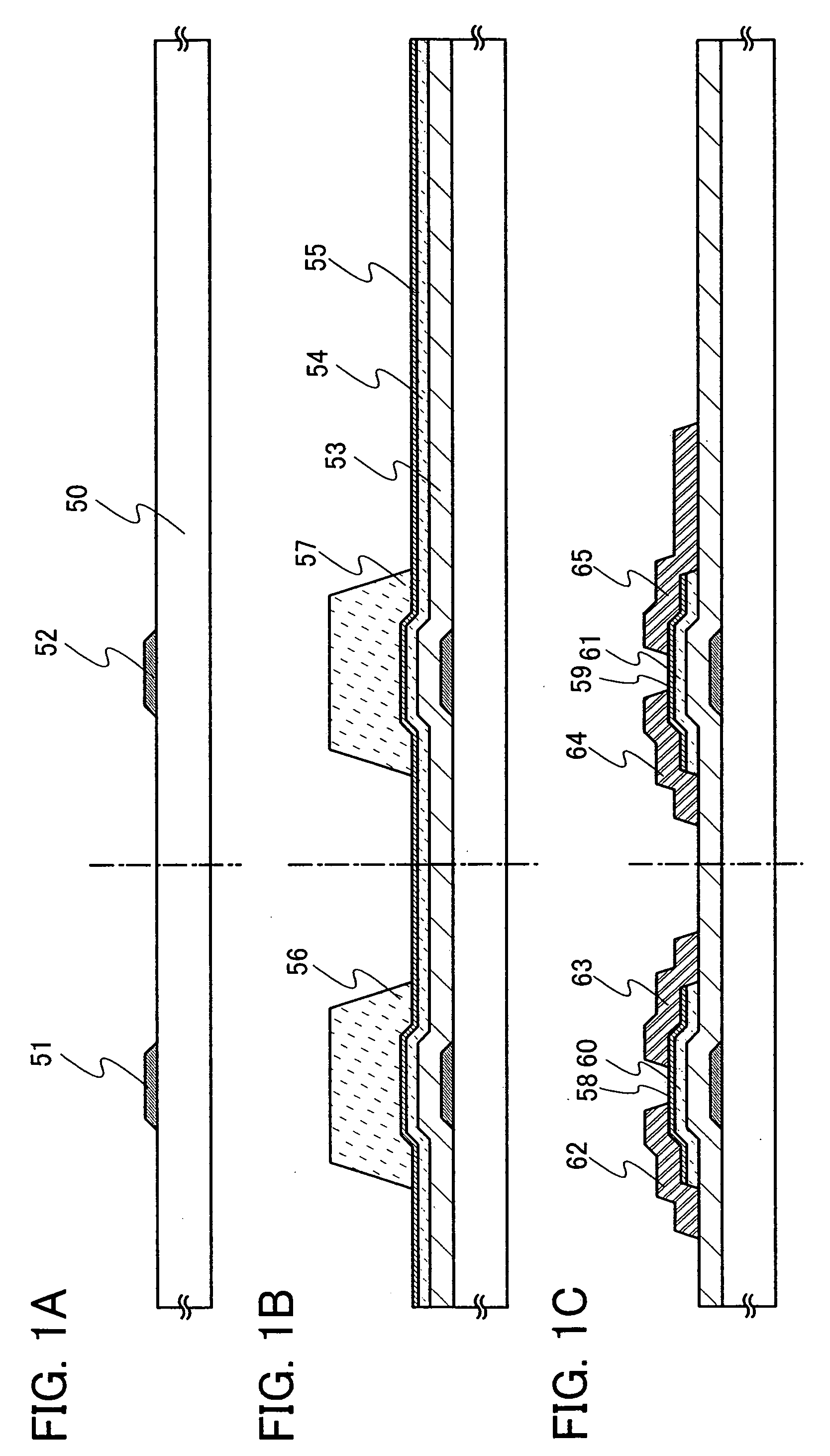
[0033]A method for manufacturing a display device of the present invention will be described. First, the description is made using a light-emitting device that is one mode of the display device. FIGS. 1A to 3C are cross-sectional views each illustrating a thin film transistor used for a driver circuit and a thin film transistor used for a pixel portion. As for a thin film transistor in which a microcrystalline semiconductor film is used, an n-type thin film transistor has higher mobility than a p-type thin film transistor; thus, an n-type thin film transistor is more suitable for a driver circuit. However, in the present invention, either an n-type or p-type thin film transistor can be used. With any polarity of a thin film transistor, it is preferable that all the thin film transistors formed over one substrate have the same polarity so that the number of manufacturing steps is reduced.

[0034]As illustrated in FIG. 1A, gate electrodes 51 and 52 are formed over a substrate 50. As the...

embodiment mode 2

[0109]This embodiment mode will describe another structure of the thin film transistor shown in Embodiment Mode 1 with reference to FIG. 12.

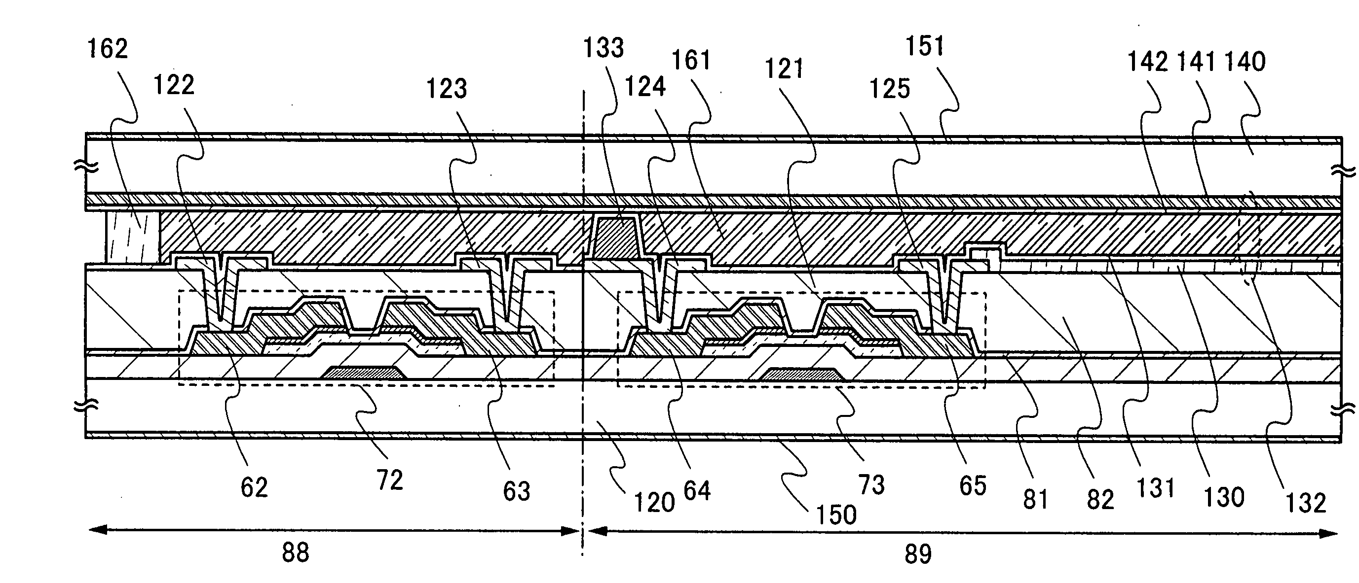
[0110]Thin film transistors 72 and 73 described in this embodiment mode has a feature that, as illustrated in FIG. 12, end portions of source electrodes 62a and 64a and end portions of source regions 66 and 68 are not in alignment, and end portions of drain electrodes 63a and 65a and end portions of drain regions 67 and 69 are not in alignment.

[0111]In this embodiment mode, using the same resist mask, a conductive film is etched by wet etching to form the source and drain electrodes 62a to 65a, and a semiconductor film to which an impurity element imparting one conductivity type is added is etched by dry etching to form the source and drain regions 66 to 69. With the structure of the source and drain electrodes 62a to 65a in this embodiment mode, the distance between the facing electrodes is widened; therefore, short-circuit between the source a...

embodiment mode 3

[0112]This embodiment mode will describe a structure of a display panel which is one mode of the display device of the present invention.

[0113]FIG. 9 illustrates a mode of a display panel in which a pixel portion 6012 formed over a substrate 6011 is connected to a signal line driver circuit 6013 which is separately formed. The pixel portion 6012 and a scanning line driver circuit 6014 are each formed using a thin film transistor which uses a microcrystalline semiconductor film. By forming the signal line driver circuit with a thin film transistor by which higher mobility can be obtained compared to a thin film transistor using the microcrystalline semiconductor film, operation of the signal line driver circuit which demands a higher driving frequency than that of the scanning line driver circuit can be stabilized. Note that the signal line driver circuit 6013 may be formed using a thin film transistor using a single-crystalline semiconductor, a thin film transistor using a polycryst...


PUM


Abstract

It is an object to provide a method for manufacturing a display device suitable for mass production without complicating a manufacturing process of a thin film transistor. A microcrystalline semiconductor film is formed by use of a microwave plasma CVD apparatus with a frequency of greater than or equal to 1 GHz using silicon hydride or silicon halide as a source gas, and a thin film transistor using the microcrystalline semiconductor film and a display element connected to the thin film transistor are formed. Since plasma which is generated using microwaves with a frequency of greater than or equal to 1 GHz has high electron density, silicon hydride or silicon halide which is a source gas can be easily dissociated, so that mass productivity of the display device can be improved.

Description

BACKGROUND OF THE INVENTION[0001]1. Field of the Invention[0002]The present invention relates to a display device including a thin film transistor at least in a pixel portion.[0003]2. Description of the Related Art[0004]In recent years, technology that is used to form a thin film transistor using a semiconductor thin film (with a thickness of from several nanometers to several hundreds of nanometers, approximately) formed over a substrate that has an insulating surface has been attracting attention. Thin film transistors are applied to a wide range of electronic devices like ICs and electro-optical devices, and prompt development of thin film transistors that are to be used as switching elements in image display devices, in particular, is being pushed.[0005]A thin film transistor using an amorphous semiconductor film, a thin film transistor using a polycrystalline semiconductor film, or the like is used as switching elements in image display devices.[0006]In addition, as switching e...

Claims


Application Information

Patent Timeline
Patent Type & Authority Applications(United States)
IPC IPC(8): H01L21/00
CPCH01L27/1214H01L29/66765H01L29/6675H01L27/127
Inventor YAMAZAKI, SHUNPEI
Owner SEMICON ENERGY LAB CO LTD
Why Eureka
Try Eureka