

Single-Step Platform for On-Chip Integration of Bio-Molecules
a bio-molecule and integrated technology, applied in the field of microarrays, can solve the problems of reduced signal-to-noise ratio, large loss of surface functionality, and no single molecular interface that meets all of the above requirements, and achieve the effect of simple and inexpensiv
- Summary
- Abstract
- Description
- Claims
- Application Information
AI Technical Summary
Benefits of technology
Problems solved by technology
Method used
Image

Examples
example 1
Preparation of an Exemplary Trifunctional Compound for Integrating Screenable Moieties to onto a Solid Substrate
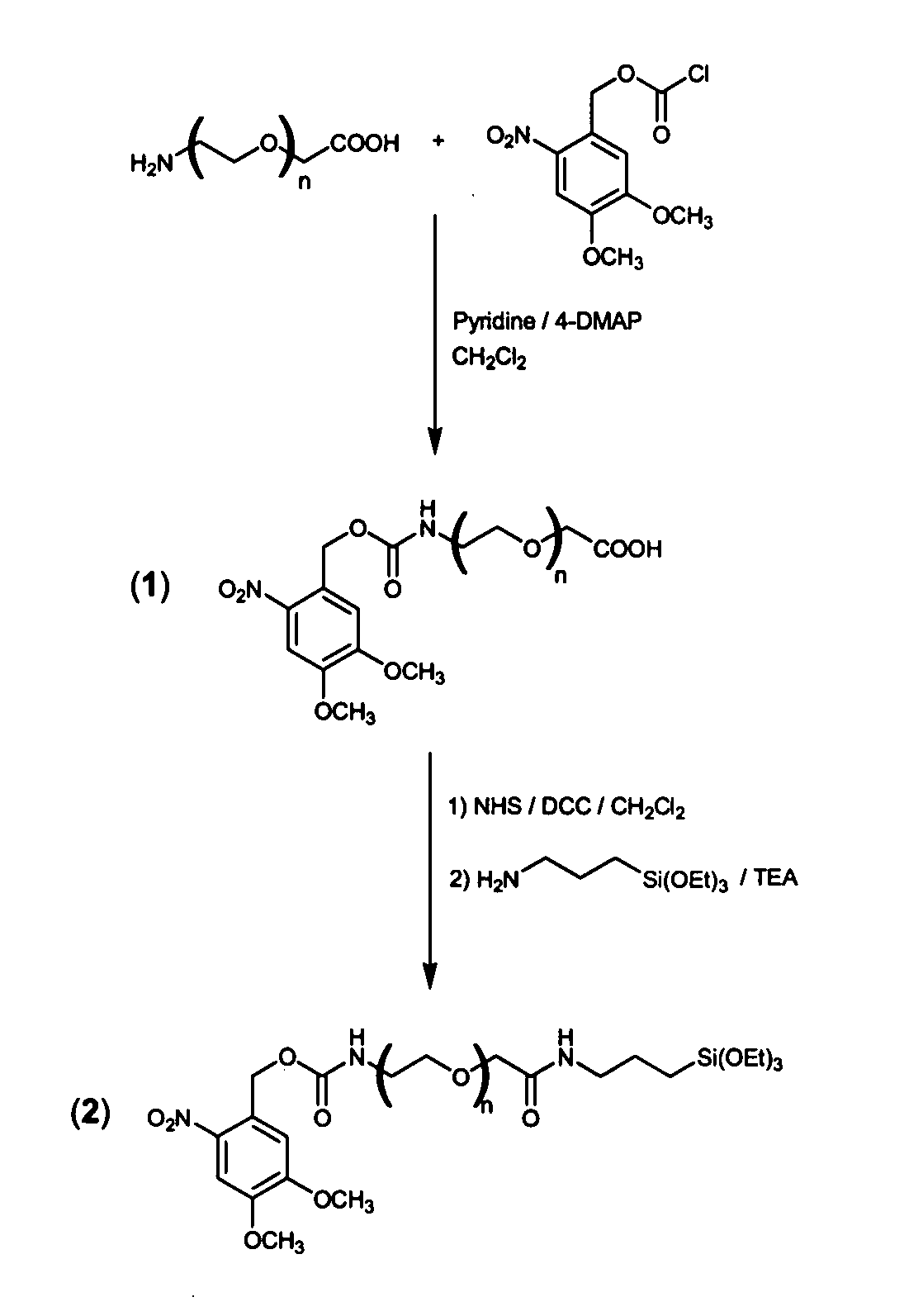
[0336]In a search for a simple-to-use, single step and inexpensive technology that integrates all previous successful approaches in one molecule, namely, a self-assembled dense monolayer that resists non-specific adsorption and supports light-directed, sub-micron immobilization of a variety of biomolecules via peptide bonds, a general chimera molecule, in which three functional modules are chemically linked together, has been designed. An exemplary such chimera molecule, also referred to herein as “daisy”, has been successfully synthesized, as shown in FIG. 1 and is further detailed hereinunder. As an exemplary starting material and backbone of the new chimera molecule, a bi-functional PEG (3400 MW) with a carboxyl and an amine at its opposite ends was selected. Amino-propyl-triethoxy-silane (APTS) was attached to the carboxyl end serving as an anchoring reactive group for...
example 2
Formation of UV-Activatable Films
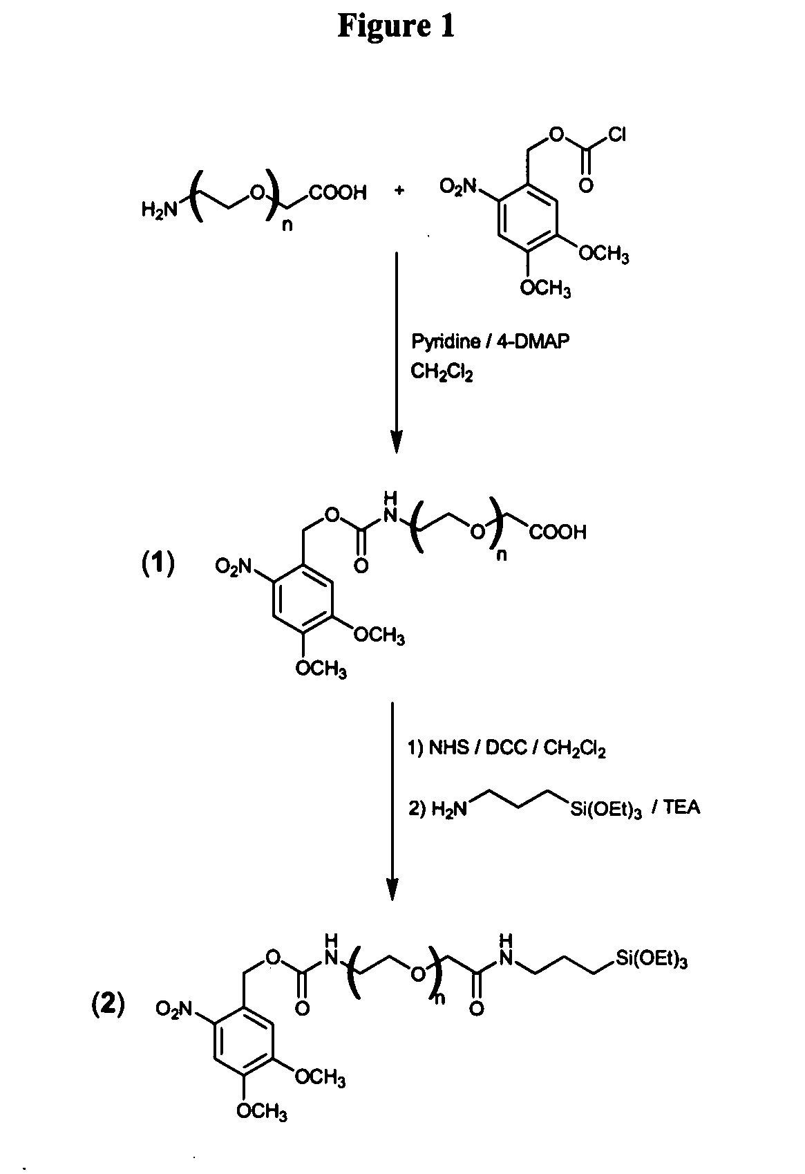
[0343]UV-activatable films (monolayers) were formed by attaching the chimera molecule (e.g., Compound 2) to a silica-coated silicon surface. The chimera molecule is preferably designed such that upon incubation with a silica-coated surface in an appropriate solvent, the molecule interacts with the SiO2 surface hydroxyl groups, so as to spontaneously form a monolayer on the surface.
[0344]Thus, Compound 2 was reacted with silicon (100) wafers coated with 100 nm of SiO2 (obtained from MEMC electronic materials, Inc.), as shown in FIG. 2, by incubation in 100 μl toluene at concentration of 0.22 mg / ml on a 1×1 cm2 wafer. A “daisy” monolayer film (Compound 3, FIG. 2) forms spontaneously on a silicon dioxide surface within few minutes of incubation in toluene.
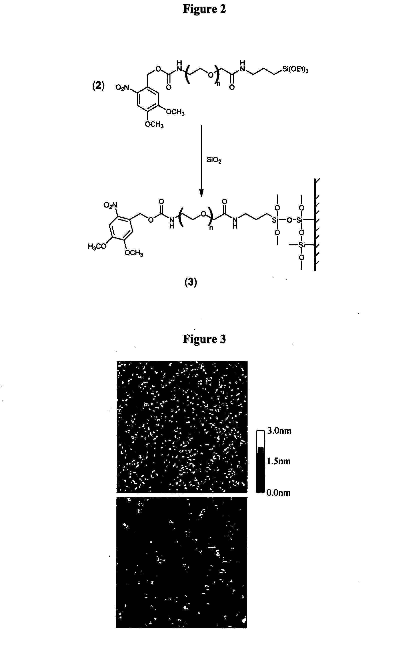
[0345]FIG. 3 presents AFM images of silica-coated (100 nm thick SiO2 layer) silicon wafers before (top) and after (bottom) incubation with Compound 2. As is shown in FIG. 3, atomic force microscope sca...
example 3
Activation of Daisy Films
[0349]The “daisy” film (Compound 3) can be readily subjected to UV-irradiation, to thereby lithographically de-protect the amine surface groups of the chimera (FIG. 4, Compound 4).
[0350]Thus, shortly after formation, the “daisy” film was used for lithographical de-protection with the 365 nm I-line of a mercury arc lamp used with a standard fluorescent optical microscope. The required pattern of amines on the daisy film was printed on transparency paper that serves as a mask placed at the field stop of the fluorescent light path. The mask was de-magnified and projected on the daisy film by the microscope objective lens [28], to produce rapid patterning molecules at sub-micron resolution, while alleviating the need for expensive contact-mode mask lithography.
[0351]Activated “daisy-coated” slides (Compound 4, FIG. 4) can be prepared in advance and stored in darkness for future use.
PUM
| Property | Measurement | Unit |
|---|---|---|
| area | aaaaa | aaaaa |
| area | aaaaa | aaaaa |
| areas | aaaaa | aaaaa |
Abstract
Description
Claims
Application Information