Glass substrate having circuit pattern and process for producing the same
a glass substrate and circuit technology, applied in the field of glass substrates with circuit patterns, can solve the problems of high production costs, low yield, and high production costs, and achieve the effects of reducing or scattering of visible light transmittance, small masks, and increasing strain stress
- Summary
- Abstract
- Description
- Claims
- Application Information
AI Technical Summary
Benefits of technology
Problems solved by technology
Method used
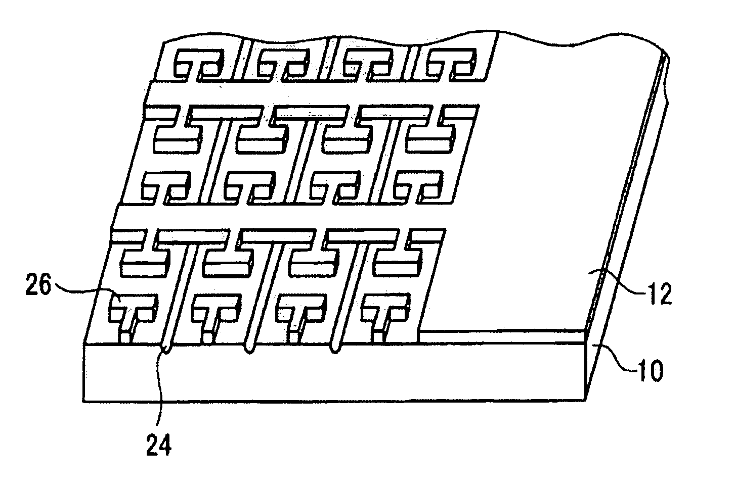
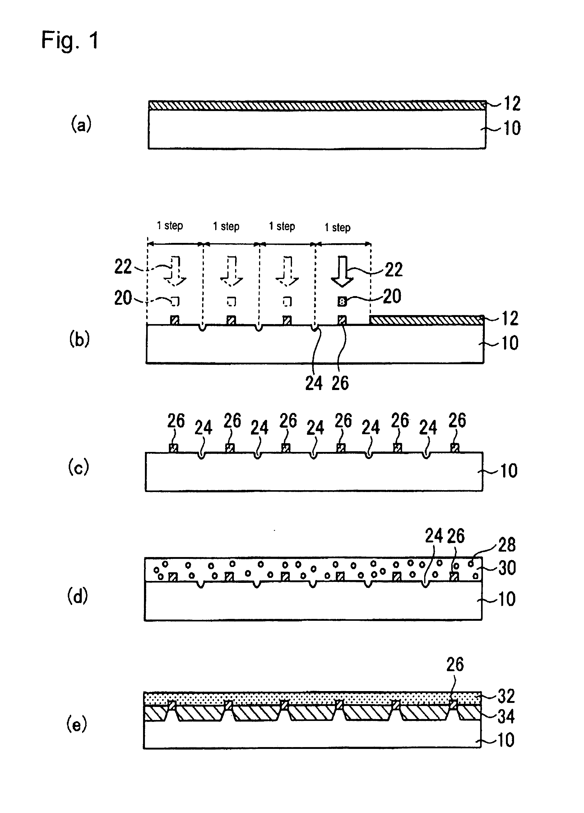
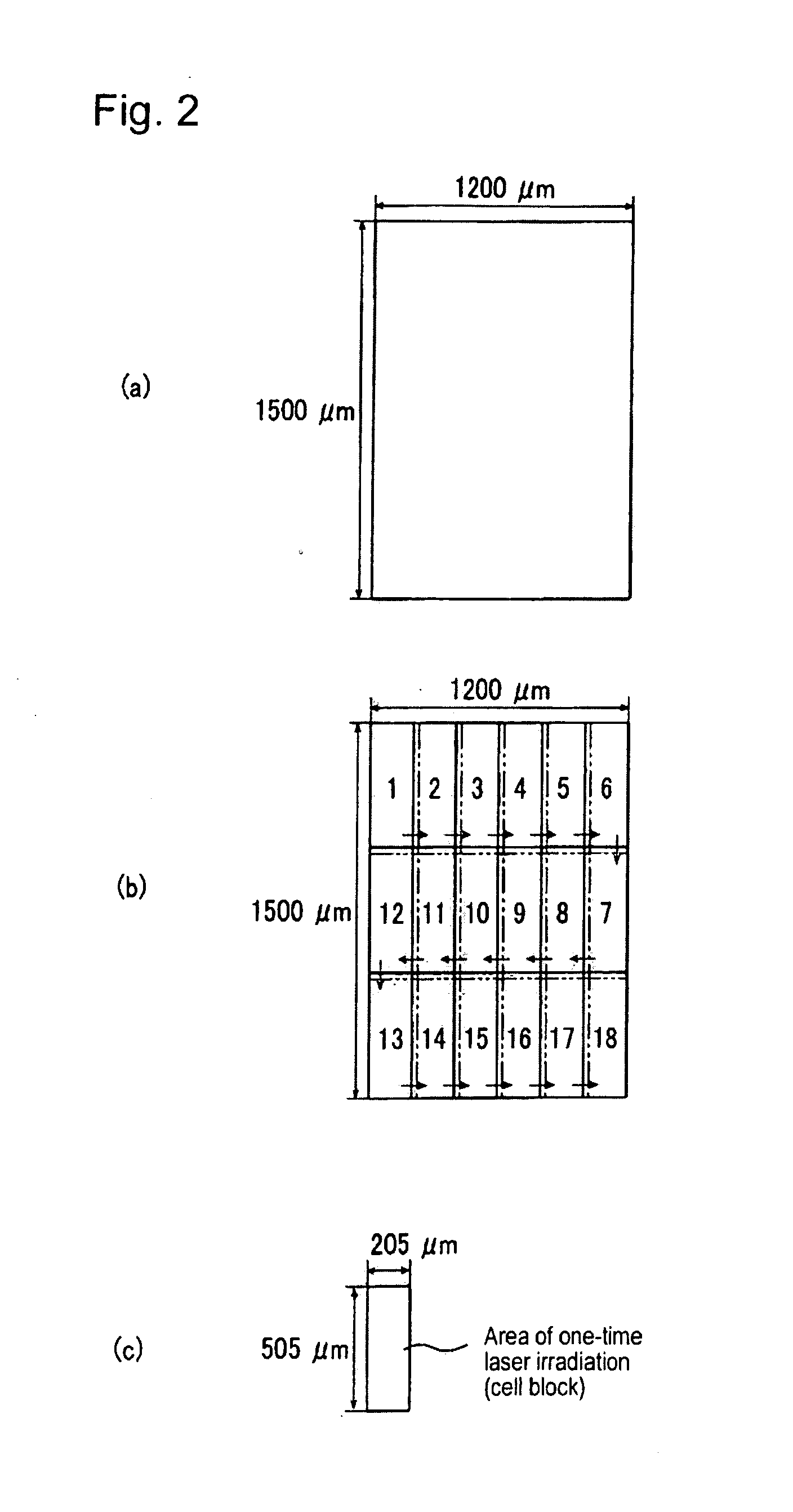
Image

Examples
example 1
[0161]A glass substrate (PD200, manufactured by Asahi Glass Co., Ltd.) of 40 mm in square and 2.8 mm in thickness was prepared. This glass substrate has an average coefficient of linear expansion at from 50 to 350° C. (JIS-R3102 (1995)) of 83×10−7 / ° C., a strain point (JIS-R3104 (1995)) of 570° C. and a softening point (JIS-R3103 (1995)) of 830° C.
[0162]This glass substrate is also hereinafter referred to as “glass substrate A”.
[0163]An antimony-doped tin oxide film was formed on one principal surface of this glass substrate A using a sputtering fabrication apparatus.
[0164]Specifically, the sputtering fabrication was carried out using, as a target, a sintered body containing 95% by mass of tin oxide and 5% by mass of antimony oxide at an initial degree of vacuum of 1.3×10⁻⁴ Pa, a glass sheet temperature of 250° C. and a degree of vacuum at the time of introduction of an argon / oxygen gas of 6.7×10⁻¹ Pa (at that time, an oxygen partial pressure was 5%).
[0165]As a result, a 300 nm-thic...
example 2
[0189]Tests were carried out under the same operations and conditions and the like as in Example 1, except for using a low-melting point glass having a softening point of 620° C. in place of the low-melting point glass having a softening point of 478° C. as used in Example 1.
[0190]Then, a cross-section of the glass substrate having a low-melting point glass formed thereon was observed by an optical microscope and an electronic microscope. As a result, the low-melting point glass had a thickness of 20 μm. Also, the compatible layer had a thickness of 0.15 μm, and it was confirmed that a laser irradiation defect was dissipated.
[0191]While the invention has been described in detail and with reference to specific embodiments thereof, it will be apparent to one skilled in the art that various changes and modifications can be made therein without departing from the spirit and scope thereof.
[0192]This application is based on Japanese Patent Application No. 2005-366410 filed Dec. 20, 2005, ...
PUM
| Property | Measurement | Unit |
|---|---|---|
| Temperature | aaaaa | aaaaa |
| Percent by mass | aaaaa | aaaaa |
| Melting point | aaaaa | aaaaa |
Abstract
Description
Claims
Application Information