Sensing Device

a technology of sensing device and target test, which is applied in the direction of optical radiation measurement, specific gravity measurement, instruments, etc., can solve the problems of large amount of test sample, and difficulty in accurately estimating the amount of change in the target test sample from the reference test sample, etc., to achieve high sensitivity and speed.

Inactive Publication Date: 2008-12-25
CANON KK
View PDF17 Cites 28 Cited by
  • Summary
  • Abstract
  • Description
  • Claims
  • Application Information

AI Technical Summary

Benefits of technology

[0008]According to the present invention, there are a plurality of transmission portions for separately propagating an electromagnetic wave including information of a test sample to be measured and an electromagnetic wave including information different from the information of the test sample. Therefore, a plurality of detection signals can be substantially simultaneously obtained. Thus, the detection signals are suitably processed (for example, comparison calculation is performed), so information of the properties or the like of the test sample can be obtained at relatively high speed with high sensitivity.

Problems solved by technology

Therefore, a large amount of test sample is necessary.
In this case, it is difficult to adjust a condition of measuring the reference test sample to the same condition as that of measuring the target test sample.
Thus, it is difficult to accurately estimate the amount of change in the target test sample from the reference test sample.

Method used


Image

  • Sensing Device
  • Sensing Device
  • Sensing Device

Examples


example 1

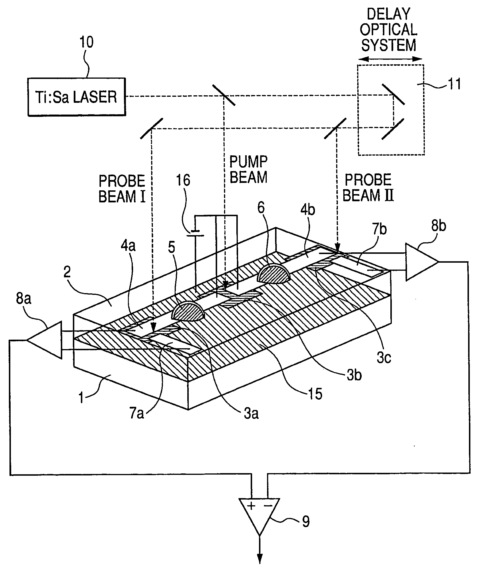
[0029]Example 1 will be described with reference to FIG. 1. In FIG. 1, a metal conductive layer 15 which becomes a ground plane and a dielectric 2 are formed on an Si substrate 1. LT-GaAs films 3a to 3c each having a thickness of approximately 2 μm and metal wirings 4a, 4b, 7a, and 7b are formed on the dielectric 2. For example, a Ti / Au layer can be used as the metal conductive layer 15, and BCB (product name: Cycloten) having a thickness of 5 μm can be used as the dielectric 2. The present invention is not limited to those.

[0030]The LT-GaAs films 3a to 3c are obtained as follows. A sacrifice layer of AlAs is grown on a GaAs substrate by an MBE method and then GaAs is grown at a low temperature of approximately 250° C. The grown GaAs film is peeled off from the AlAs layer and thus can be bonded onto the BCB dielectric 2. When only the LT-GaAs film 3b of the transferred LT-GaAs films is to be electrically connected with the ground plane 15, a through wiring (not shown) is formed. A v...

example 2

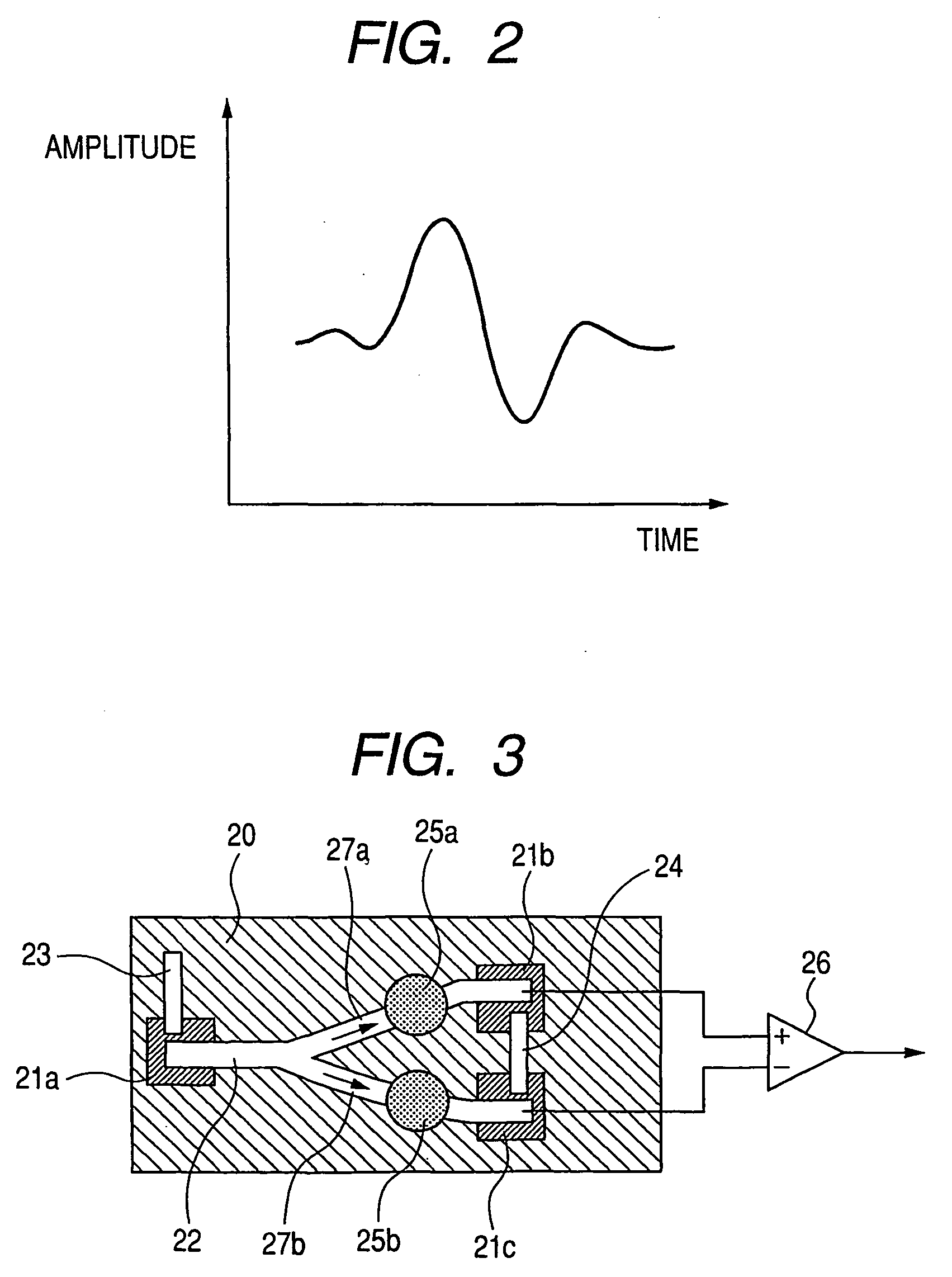
[0036]An operation in Example 2 of the present invention is substantially identical to that in Example 1. A different point is that a metal wiring 22 is branched at a point thereof to form Y-branch transmission paths 27a and 27b as shown in a plan view of FIG. 3. At a generation portion 21a, a laser beam is applied to a gap portion between the wirings 22 and 23. The laser beam may be an ultra-short pulse laser beam of approximately 100 fsec as in the case of Example 1. An oscillating frequency difference of a THz order may be caused between two semiconductor lasers oscillated in a 830 nm band to apply a THz continuous wave of a single frequency as its beat signal.

[0037]A terahertz wave from the generation portion 21a is divided into two by the Y-branch transmission paths 27a and 27b. The two waves reach detection regions 21b and 21c in which photoconductive switch elements are formed to perform signal detection. At this time, balance reception using a differential amplifier 26 is pe...

example 3

[0038]Example 3 of the present invention uses a current injection terahertz oscillator element. Unlike the above-mentioned examples, it is unnecessary to apply a laser beam from the outside, so size of the sensing device can be significantly reduced. An optical adjustment mechanism is unnecessary, so cost can be reduced. FIG. 4 is a plan view showing the terahertz oscillator element. In this example, the transmission paths are formed as coplanar strip lines 41 and 42 having two lines provided on a surface of a substrate 40. Each of the lines 41 and 42 has a distributed Bragg reflector (DBR) structure to resonate at a specific frequency and also serves as a resonator for an oscillator 43. The oscillator 43 is designed such that a resonant tunnel diode (RTD) is used for a gain structure and a maximum gain peak is obtained at the vicinity of 1 THz. Therefore, even in the case of the DBR, a diffraction grating is formed such that a reflection strength becomes stronger at the vicinity of...


PUM

PropertyMeasurementUnit
thicknessaaaaaaaaaa
thicknessaaaaaaaaaa
temperatureaaaaaaaaaa

Abstract

The present invention provides a sensing device for obtaining information of a test sample using an electromagnetic wave including a frequency region within a frequency region of 30 GHz to 30 THz, the sensing device comprising an electromagnetic wave transmitting portion including a plurality of transmission portions (4a, 4b) for propagating electromagnetic waves and detection portions (3a, 3c) for receiving and detecting the electromagnetic waves from the plurality of transmission portions (4a, 4b), in which at least one of the plurality of transmission portions (4a, 4b) is constructed such that the test sample (5, 6) can be placed in a portion affected by an electromagnetic wave propagating therethrough.

Description

TECHNICAL FIELD[0001]The present invention relates to a sensing device and method for obtaining information of, for example, properties of a target test sample using an electromagnetic wave including a frequency region principally within a millimeter-wave to terahertz-wave region (30 GHz to 30 THz).BACKGROUND ART[0002]In recent years, nondestructive sensing techniques using an electromagnetic wave of millimeter-wave to terahertz (THz) wave frequencies (30 GHz to 30 THz) have been under development. An example of techniques now under development in application fields of the electromagnetic wave of such a frequency band is an imaging technique using a safe fluoroscopic apparatus alternative to an X-ray fluoroscope. In addition, examples of techniques now under development include a spectral technique for obtaining an absorption spectrum or complex dielectric constant of a material to examine the bonding state therein, a technique for analyzing biomolecules, and a technique for estimat...

Claims


Application Information

Patent Timeline
Patent Type & Authority Applications(United States)
IPC IPC(8): G01H5/00G01N21/35G01N21/3563G01N21/3586
CPCG01N21/276G01N21/3581G01N21/3577
Inventor OUCHI, TOSHIHIKO
Owner CANON KK
Why Eureka
Try Eureka