Eureka AIR delivers breakthrough ideas for toughest innovation challenges, trusted by R&D personnel around the world.

Plasma enhanced cyclic deposition method of metal silicon nitride film

a metal silicon nitride and cyclic deposition technology, which is applied in the direction of coatings, chemical vapor deposition coatings, metallic material coating processes, etc., can solve the problems of poor step coverage of deposited metal nitride films, insufficient sputtering methods to form films, and poor cyclic deposition of films. , to achieve the effect of improving the cyclic deposition of films

Inactive Publication Date: 2008-12-25
VERSUM MATERIALS US LLC
View PDF22 Cites 44 Cited by
  • Summary
  • Abstract
  • Description
  • Claims
  • Application Information

AI Technical Summary

Benefits of technology

[0008]In another embodiment, the invention provides an improved cyclic deposition of films by using preferred precursors under plasma atmosphere.

Problems solved by technology

With the trend, a sputtering method is inadequate to form a film with a uniform thickness.
CVD is typically used to form a uniform film thickness but not enough to meet the requirement of good step coverage in a high-aspect ratio structure of devices.
It is known that the deposited metal nitride films have bad step coverage due to the reaction between gaseous alkylamido metal compound and ammonia gas, particularly in the case of using an alkylamido metal precursor to chemically deposit metal nitride films.
Using a metal chloride precursor, a silicon source such as silane, and ammonia, it requires a very high temperature process up to about 1000° C. which makes this process undesirable for certain substrate.

Method used


Image

  • Plasma enhanced cyclic deposition method of metal silicon nitride film
  • Plasma enhanced cyclic deposition method of metal silicon nitride film
  • Plasma enhanced cyclic deposition method of metal silicon nitride film

Examples


example 1

Preparation of Titanium Silicon Nitride (TiSiN) Films at 450° C. by PEALD

[0060]The cycle was comprised of sequential supplies of TDMAT bubbled by an Ar carrier gas at a flow rate of 25 sccm for various pulsing times; an Ar purge gas at a flow rate of 500 sccm for 5 seconds; an ammonia gas at a flow rate of 100 sccm for 5 seconds during RF plasma generation; an Ar purge gas at a flow rate of 500 sccm for 5 seconds; BTBAS bubbled by an Ar carrier gas at a flow rate of 25 sccm for various pulsing times; an Ar purge gas at a flow rate of 500 sccm for 5 seconds; an ammonia gas at a flow rate of 100 sccm for 5 seconds during RF plasma generation; and an Ar purge gas at a flow rate of 500 sccm for 5 seconds. Process chamber pressure was about 1.0 Torr and the heater temperature 450° C. corresponded to the wafer temperature, 395° C.

[0061]Keeping the total precursor flow amount at each condition the same as 3.5 seconds, TDMAT / BTBAS pulsing time was changed to (0.5 seconds / 3 seconds), (1.75 s...

example 2

Preparation of Titanium Silicon Nitride (TiSiN) Films at 250° C. by PEALD

[0066]Except for the heater temperature being 250° C., the cycle was the same as that in above example 1. The heater temperature of 250° C. corresponded to the wafer temperature of 235° C.

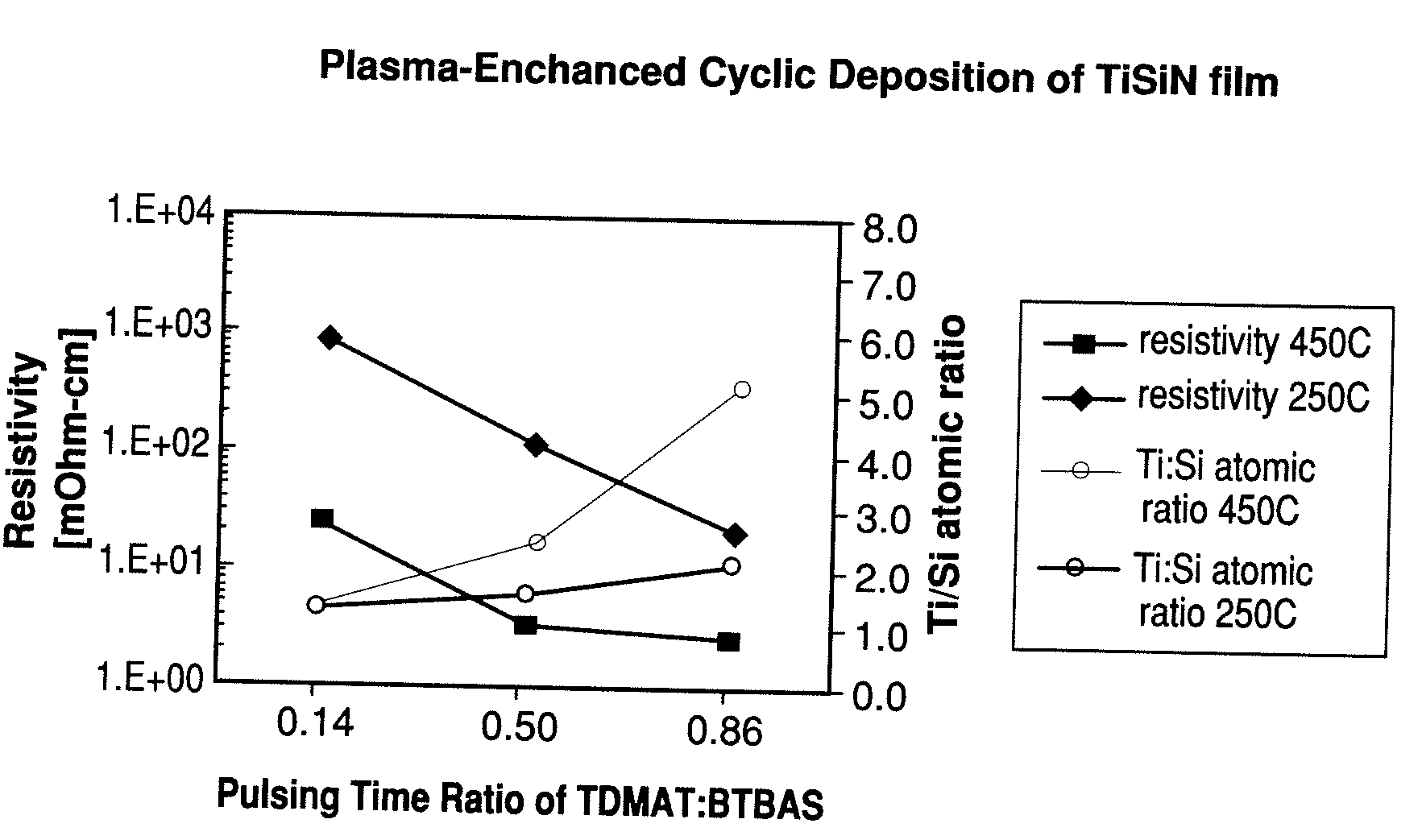
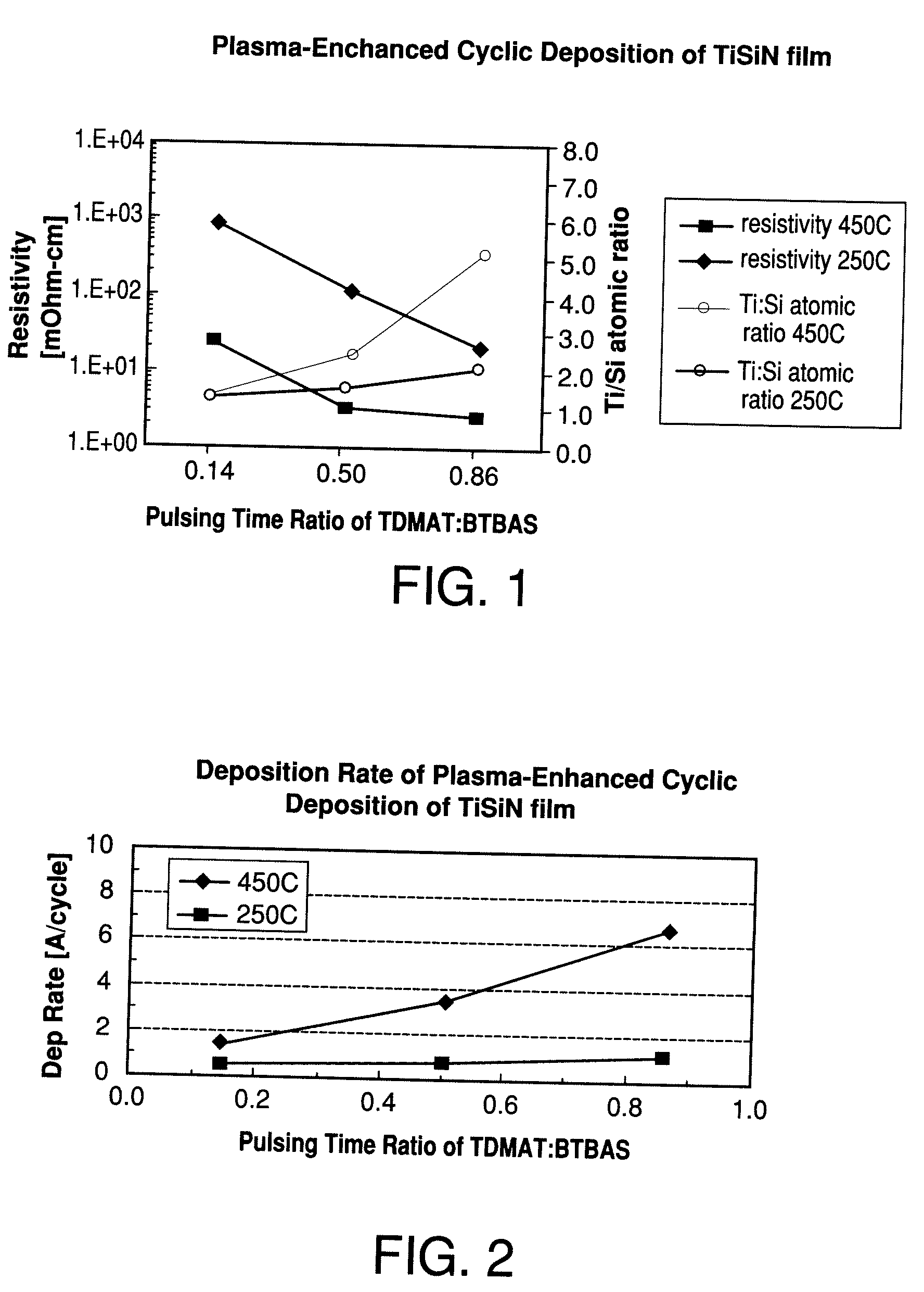
[0067]FIGS. 1 and 2 illustrate the results of the above test.

[0068]As illustrated in FIG. 1, the resistivities for the above conditions were 915.1, 123.5, and 22.5 mOhm-cm, respectively, and RBS analysis showed Ti / Si ratio, 1.3, 1.6, and 2.1, respectively.

[0069]Also, as illustrated in FIG. 2, the deposition rates for the above conditions were 0.6, 0.8, and 1.1Å / cycle, respectively, which reflected that the above conditions were in the ALD region. In other words, metal silicon nitride films, which can be grown at a low process temperature, can be provided.

example 3

Preparation of Titanium Silicon Nitride (TiSiN) Films at 250° C. by the Thermal ALD

[0070]The cycle was comprised of sequential supplies of TDMAT bubbled by an Ar carrier gas at a flow rate of 25 sccm for various pulsing times; an Ar purge gas at a flow rate of 500 sccm for 5 seconds; an ammonia gas at a flow rate of 100 sccm for 5 seconds without RF plasma generation; an Ar purge gas at a flow rate of 500 sccm for 5 seconds; BTBAS bubbled by an Ar carrier gas at a flow rate of 25 sccm for various pulsing times; an Ar purge gas at a flow rate of 500 sccm for 5 seconds; an ammonia gas at a flow rate of 100 sccm for 5 seconds without RF plasma generation; and an Ar purge gas at a flow rate of 500 sccm for 5 seconds. Process chamber pressure was about 1.0 Torr, and the heater temperature of 250° C. corresponded to the wafer temperature of 235° C.

[0071]Keeping the total precursor flow amount at each condition the same as 3.5 seconds, TDMAT / BTBAS pulsing time was changed to (0.5 seconds / 3...


PUM

PropertyMeasurementUnit
temperatureaaaaaaaaaa
temperaturesaaaaaaaaaa

Abstract

The present invention relates to a method for forming a metal silicon nitride film according to a cyclic film deposition under plasma atmosphere with a metal amide, a silicon precursor, and a nitrogen source gas as precursors. The deposition method for forming a metal silicon nitride film on a substrate comprises steps of: pulsing a metal amide precursor; purging away the unreacted metal amide; introducing nitrogen source gas into reaction chamber under plasma atmosphere; purging away the unreacted nitrogen source gas; pulsing a silicon precursor; purging away the unreacted silicon precursor; introducing nitrogen source gas into reaction chamber under plasma atmosphere; and purging away the unreacted nitrogen source gas.

Description

BACKGROUND OF THE INVENTION[0001]The present invention relates to a method for forming a metal silicon nitride film according to a cyclic film deposition under plasma atmosphere with a metal amide, a silicon precursor, and a nitrogen source gas as precursors.[0002]Phase change memory (PRAM) devices use phase change materials that can be electrically switched between an amorphous and a crystalline state. Typical materials suitable for such an application include various chalcogenide elements such as germanium, antimony and tellurium. In order to induce a phase change, a chalcogenide material should be heated up by a heater. There are many potential heating materials such as titanium nitride (TiN), titanium aluminium nitride (TiAlN), titanium silicon nitride (TiSiN), tantalum silicon nitride (TaSiN), and so on.[0003]The widely studied deposition techniques for preparing those films are a physical vapor deposition (PVD), i.e., a sputtering, and a chemical vapor deposition (CVD) techniq...

Claims


Application Information

Patent Timeline
Patent Type & Authority Applications(United States)
IPC IPC(8): H01L21/285C23C16/34
CPCC23C16/34C23C16/45531C23C16/45542C23C16/45553C23C16/50
Inventor KIM, MIN-KYUNGHAN, YANG-SUKKIM, MOO-SUNGYANG, SANG-HYUNLEI, XINJIAN
Owner VERSUM MATERIALS US LLC
Why Eureka
Eureka Blog
Learn More