Non-Volatile Memory Device and Method of Fabricating the Same

Active Publication Date: 2009-01-01
COLUMBA TECH INC
View PDF10 Cites 11 Cited by
  • Summary
  • Abstract
  • Description
  • Claims
  • Application Information

AI Technical Summary

Benefits of technology

[0011]According to an embodiment, provided is a non-volatile memory device capable of lowering a program voltage by using a tunneling tip. Because the program voltage is lowered, the size of a memory cell can be reduced and its structure becomes simpler. There

Problems solved by technology

However, because the floating gate cell requires a high voltage during programming or erasing operations, and because it is difficult

Method used


Image

  • Non-Volatile Memory Device and Method of Fabricating the Same
  • Non-Volatile Memory Device and Method of Fabricating the Same
  • Non-Volatile Memory Device and Method of Fabricating the Same

Examples


Example

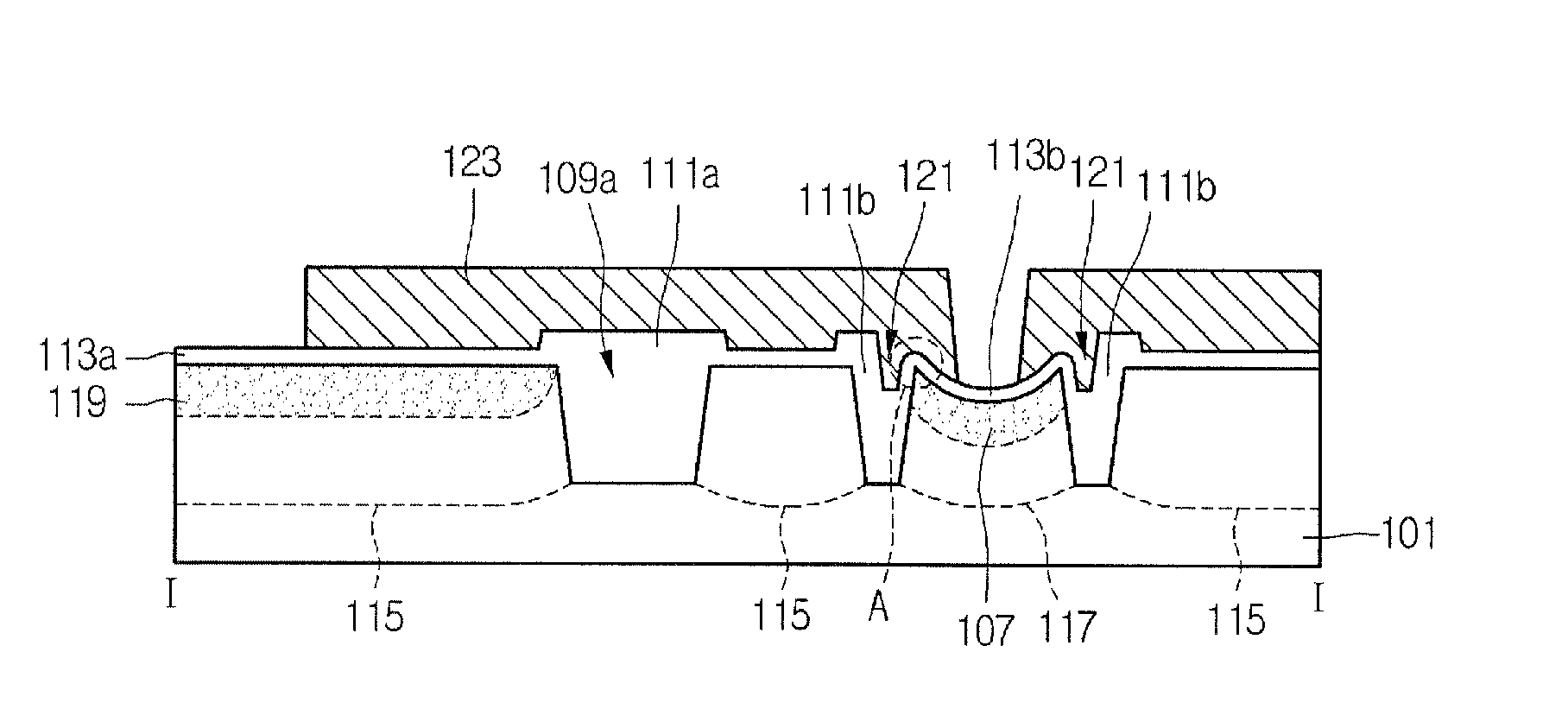
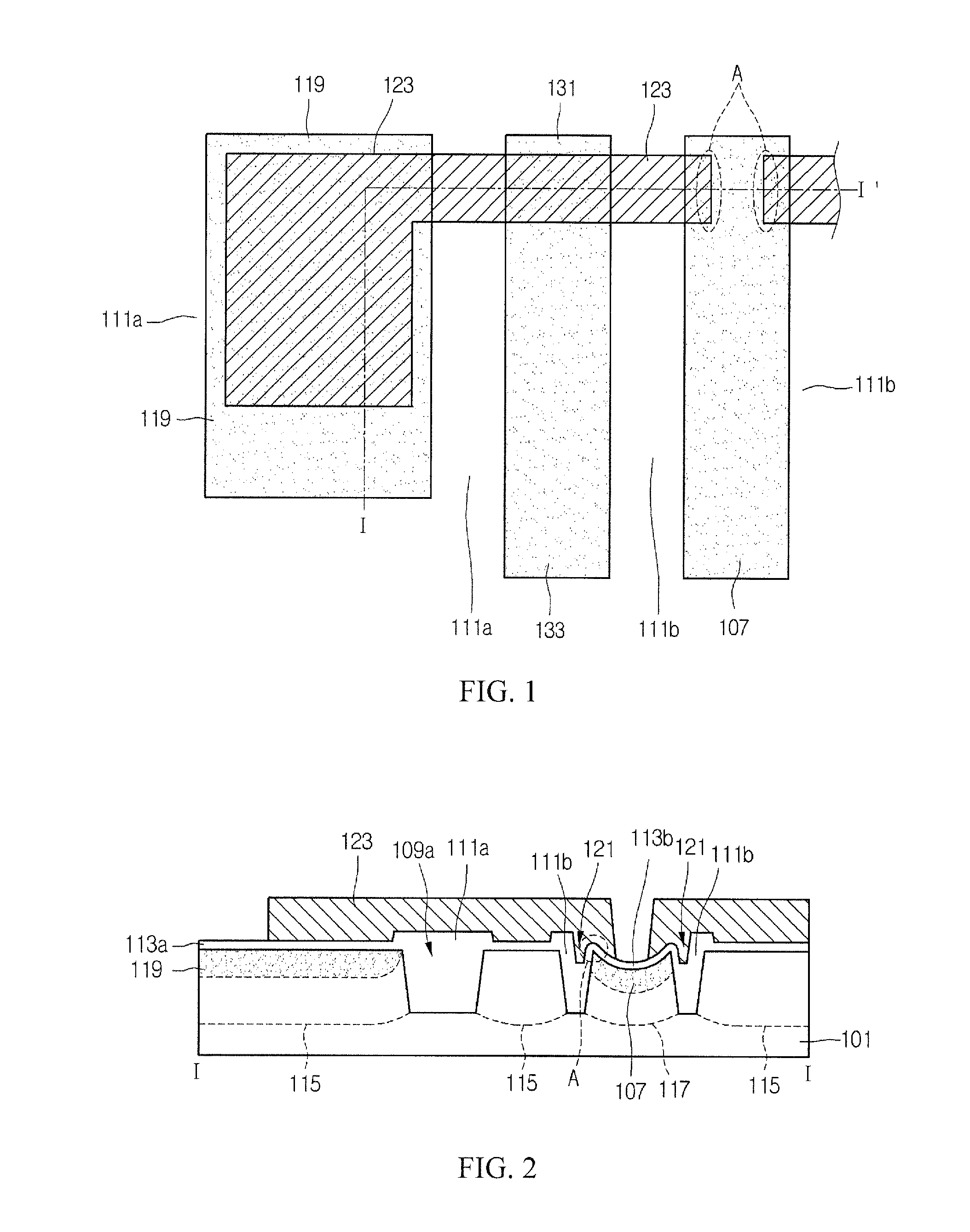
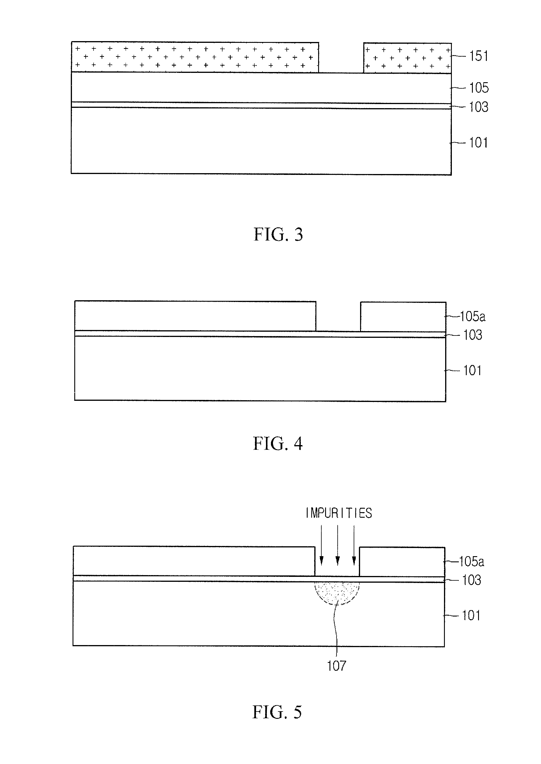
[0017]Hereinafter, a method of fabricating a semiconductor device according to embodiments will now be described in detail with reference to the accompanying drawing. It should be understood that numerous other additions, deletions, modifications, and embodiments can be suggested by those skilled in the art upon review of the subject disclosure that will fall within the spirit and scope of the principles of this disclosure.

[0018]In addition, it will also be understood that when terms such as “first” and “second” are used to describe members, the members are not limited by these terms. For example, a plurality of members may be provided. Therefore, when the terms “first” and “second” are used, it will be apparent that the plurality of members may be provided. In addition, the terms “first” and “second” can be selectively or interchangeably used for the members. In the figures, a dimension of each of elements is exaggerated for clarity of illustration, and the dimension of each of the...


PUM


Abstract

Provided are a non-volatile memory device and a method of fabricating the same. The non-volatile memory device comprises: a control gate region formed by doping a semiconductor substrate with second impurities; an electron injection region formed by doping the semiconductor substrate with first impurities, where a top surface of the electron injection region includes a tip portion at an edge; a floating gate electrode covering at least a portion of the control gate region and the tip portion of the electron injection region; a first tunnel oxide layer interposed between the floating gate electrode and the control gate region; a second tunnel oxide layer interposed between the floating gate electrode and the electron injection region; a trench surrounding the electron injection region in the semiconductor substrate; and a device isolation layer pattern filled in the trench.

Description

RELATED APPLICATION[0001]The application claims priority under 35 U.S.C. §119(e) of Korean Patent Application No. 10-2007-0062643 filed on Jun. 26, 2007, which is hereby incorporated by reference in its entirety.BACKGROUND[0002]Because a non-volatile memory retains stored data even when there is no power supply, it is often used for data storage in systems such as a personal computer (PC) basic input / output system (BIOS), a set-top box, a printer, and a network server. Recently, non-volatile memory is being used in digital cameras and mobile phones.[0003]One common non-volatile memory is an electrically erasable programmable read-only memory (EEPROM) flash memory device. In the EEPROM flash memory device, during a programming operation, channel hot electrons form in a drain region to accumulate electrons in a floating gate, such that a threshold voltage of a cell transistor is increased.[0004]Then, during an erasing operation, the EEPROM flash memory device generates a high voltage ...

Claims


Application Information

Patent Timeline
IPC IPC(8): H01L29/788H01L21/336
CPCH01L21/28273H01L27/115H01L29/7881H01L29/42336H01L27/11521H01L29/40114H10B69/00H10B41/30H01L21/76838
Inventor PARK, SUNG KUN
Owner COLUMBA TECH INC
Why Eureka
Try Eureka