Method of manufacturing semiconductor device

a manufacturing method and semiconductor technology, applied in the direction of organic semiconductor devices, solid-state devices, transistors, etc., can solve the problems of plastic film exposure, plastic film deformation, plastic film exposure, etc., and achieve the effect of reducing costs and smooth separation process

Inactive Publication Date: 2009-01-01
SEMICON ENERGY LAB CO LTD
View PDF8 Cites 100 Cited by
  • Summary
  • Abstract
  • Description
  • Claims
  • Application Information

AI Technical Summary

Benefits of technology

[0032]By the present invention, a separation process can be performed smoothly, even if a substrate with a large area, where the length of the diagonal of the substrate exceeds 1 meter, is used. In addition, by provision of an organic compound film between a molybdenum oxide film and semiconductor elements, the organic compound film can be made to function as a support for the semiconductor device. For this reason, a support substrate used to support the semiconductor device need not be formed unnecessarily, and costs can be reduced.

Problems solved by technology

Furthermore, when thin film transistors formed using amorphous semiconductor films or the like and thin film transistors formed using organic semiconductor films are directly formed over plastic films, there is a risk that the plastic films will be exposed to solvents or etching gases that are used in the course of the thin film transistor fabrication process and that the quality of the plastic films themselves will change because of this exposure.
In addition, when thin film transistors formed using ZnO are directly formed over plastic films, if the plastic films are irradiated by plasmas that are generated by a sputtering method or the like, the plastic films themselves will become deformed.
Moreover, there is a possibility that moisture or the like will be absorbed into the plastic films in the course of the thin film transistor fabrication process or that the elements will be contaminated by emission.
Additionally, because heat resistance is lower and the degree of heat-induced expansion and contraction higher for plastic films than for glass substrates, carefully controlling the process temperature of each step of the fabrication process is difficult.
However, with a roll-to-roll method, existing semiconductor manufacturing equipment cannot be used.
In addition, the level of accuracy for alignment is low, and microfabrication is difficult.
As a result, fabrication of semiconductor devices, in which characteristics equivalent to those of conventional semiconductor devices formed using glass substrates are obtained, at high yield is difficult.

Method used


Image

  • Method of manufacturing semiconductor device
  • Method of manufacturing semiconductor device
  • Method of manufacturing semiconductor device

Examples


embodiment mode 1

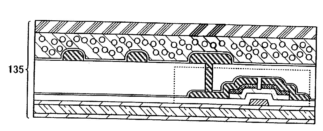
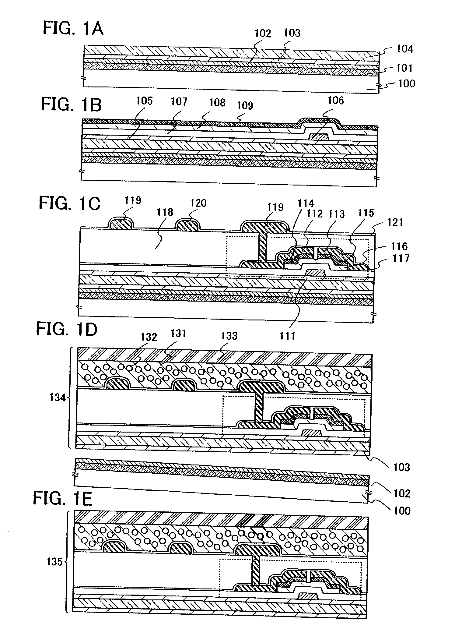
[0051]Here, an example in which a liquid crystal display device is fabricated will be described using FIGS. 1A to 1E.

[0052]A molybdenum film 101 is formed over a substrate 100. A glass substrate is used for the substrate 100. Furthermore, for the molybdenum film 101, a molybdenum film with a thickness of from 30 nm to 200 nm obtained by a sputtering method is used. It is to be noted that, because there are cases where the substrate is locked in place in a sputtering method, the film thickness of the molybdenum film in the vicinity of the edges of the substrate easily becomes uneven. For this reason, it is preferable that the edges of the molybdenum film be removed by dry etching.

[0053]Next, a molybdenum oxide film 102 is formed over the molybdenum film 101. The molybdenum oxide film 102 can be formed by an evaporation method. Alternatively, the molybdenum oxide film 102 may be formed in contact with the molybdenum film 101; the surface of the molybdenum film 101 may be oxidized, and...

embodiment mode 2

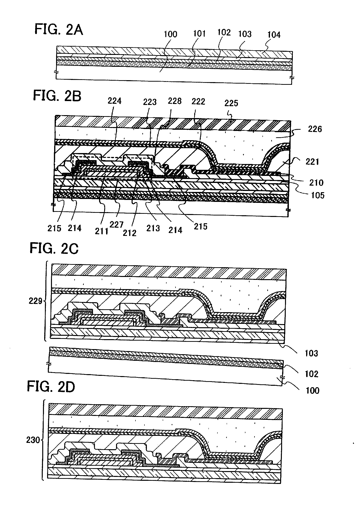
[0076]Here, an example in which an active matrix light-emitting device that uses organic thin film transistors is fabricated will be described using FIGS. 2A to 2D.

[0077]As in Embodiment Mode 1, the molybdenum film 101 is formed over the substrate 100, the molybdenum oxide film 102 is formed over the molybdenum film 101, the nonmetal inorganic film 103 is formed over the molybdenum oxide film 102, and the organic compound film 104 is formed over the nonmetal inorganic film 103. A cross-sectional process diagram of what is obtained after processes up to this stage have been completed is shown in FIG. 2A.

[0078]Next, the inorganic insulating film 105 may be formed over the organic compound film 104. Subsequently, a conductive layer 211 that is to be used as a gate electrode is formed over the organic compound film 104 or over the inorganic insulating film 105. For a material used in the conductive layer 211, a metal that is made to be insulative by either nitridation or oxidation or by...

embodiment mode 3

[0105]Here, an example in which a passive matrix light-emitting device is fabricated over a flexible substrate will be described using FIGS. 5A to 5C, FIG. 6, FIG. 7, FIGS. 8A and 8B, and FIG. 9.

[0106]A passive matrix (simple matrix) light-emitting device has a structure in which a plurality of anodes is provided in parallel stripe form (band form) and a plurality of cathodes is provided in parallel stripe form so that the plurality of anodes and the plurality of cathodes are perpendicular to each other and a structure in which a light-emitting layer or a fluorescent layer is inserted at an intersection of each of the plurality of anodes and plurality of cathodes. Consequently, a pixel located at an intersection of a selected anode (an anode to which a voltage is applied) and a selected cathode comes to be lit up.

[0107]FIG. 5A is a diagram illustrating a top view of a pixel portion before a flexible substrate is attached to a second electrode 516 of a light-emitting element. FIG. 5B...


PUM

PropertyMeasurementUnit
temperatureaaaaaaaaaa
thicknessaaaaaaaaaa

Abstract

An object of the invention is to provide a method for manufacturing semiconductor devices that are flexible in which elements fabricated using a comparatively low-temperature (less than 500° C.) process are separated from a substrate. After a molybdenum film is formed over a glass substrate, a molybdenum oxide film is formed over the molybdenum film, a nonmetal inorganic film and an organic compound film are stacked over the molybdenum oxide film, and elements fabricated by a comparatively low-temperature (less than 500° C.) process are formed using existing manufacturing equipment for large glass substrates, the elements are separated from the glass substrate.

Description

BACKGROUND OF THE INVENTION[0001]1. Field of the Invention[0002]The present invention relates to a method of manufacturing semiconductor devices including thin film transistors, light-emitting elements, passive elements, and the like. Furthermore, the present invention relates to electro-optical devices represented by liquid crystal display panels, light-emitting display devices that have light-emitting elements, and electronic devices in which IC tags, by which information can be transmitted and received wirelessly, are mounted as components.[0003]It is to be noted that “semiconductor device” in the present specification refers to a general device that can function as a semiconductor device using semiconductor characteristics, and electro-optical devices, light-emitting devices, semiconductor circuits, IC tags, and electronic devices can all be considered semiconductor devices.[0004]2. Description of the Related Art[0005]In recent years, technology that is used to form thin film tr...

Claims


Application Information

Patent Timeline
Patent Type & Authority Applications(United States)
IPC IPC(8): H01L51/40
CPCH01L21/2026H01L27/1214H01L27/1266H01L27/283H01L27/3274H01L28/40H01L27/12H01L29/7869H01L51/003H01L51/56H01L2227/323H01L2251/5338H01L29/78603H01L21/02488H01L21/02491H01L21/02505H01L21/02686H01L21/02532H01L21/02565H01L29/24H01L29/42356H01L29/45H01L29/4908H01L29/495H01L29/66969H10K19/10H10K59/124H10K59/125H10K71/80H10K59/1201H10K71/00H10K2102/311H01L21/76251
Inventor JINBO, YASUHIROISA, TOSHIYUKIHONDA, TATSUYA
Owner SEMICON ENERGY LAB CO LTD
Why Eureka
Try Eureka