Method for Etching Single Wafer

a single-wallet etching technology, applied in the field of methods, can solve the problems of affecting the etching effect of the etching amount is not enough, so as to improve the degree of freedom to control the distribution of etching amount on the surface of the wafer, improve the etching effect, and improve the effect of etching

Active Publication Date: 2009-01-01
SUMCO CORP
View PDF11 Cites 22 Cited by
  • Summary
  • Abstract
  • Description
  • Claims
  • Application Information

AI Technical Summary

Benefits of technology

[0018]As described above, according to the present invention, a plurality of etching solution supply nozzles are disposed above and opposite to the front surface of the wafer at different portions in the radial direction of the wafer, respectively and one or more conditions selected from the group consisting of temperatures, kinds, and supply flow rates of etching solutions from the plurality of etching solution supply nozzles are then changed. Therefore, an optimum etching solution, where the temperature, kind, or supply flow rate thereof are adjusted, is supplied to each part of the wafer from the plurality of etching solution supply nozzles. As a result, the degree of freedom to control the distribution of etching amount on the surface of the wafer can be increased and the wafer can be effectively provided with high flatness, thereby allowing the wafer to be easily subjected to the subsequent step of grinding.
[0019]In addition, the temperature of the first etching solution supplied from the first supply nozzle to the center of the front surface of the wafer is higher than the temperature of the second etching solution supplied from the second supply nozzle to the periphery of the front surface of the wafer, so that the etching rate of the wafer with the first etching solution can be higher than the etching rate of the wafer with the second etching solution. As a result, the excessive etching of the periphery of the wafer can be repaired, thereby efficiently providing the wafer with high flatness.
[0020]In addition, an etching solution used as the first etching solution supplied from the first supply nozzle to the center of the front surface of the wafer has a higher etching rate than that of the second etching solution supplied from the second supply nozzle to the periphery of the front surface of the wafer, so that the etching rate of the wafer with the first etching solution can be higher than the etching rate of the wafer with the second etching solution. As a result, the excessive etching of the periphery of the wafer can be repaired, thereby efficiently providing the wafer with high flatness.
[0021]Furthermore, the supply flow rate of the first etching solution supplied from the first supply nozzle to the center of the front surface of the wafer is higher than that of the second etching solution supplied from the second supply nozzle to the periphery of the front surface of the wafer, so that the etching rate of the wafer with the first etching solution can be higher than the etching rate of the wafer with the second etching solution. As a result, the excessive etching of the periphery of the wafer can be repaired, thereby efficiently providing the wafer with high flatness.

Problems solved by technology

In the process for device production, such a processing-strained layer causes crystal defects, such as slip dislocation, and the mechanical strength of the wafer is then decreased.
In addition, it has adverse effects on electric characteristics.
Furthermore, most of the etching solution supplied is blown off from the edge thereof by centrifugal force and then collected into a cup or the like arranged on an etching device.

Method used


Image

  • Method for Etching Single Wafer
  • Method for Etching Single Wafer
  • Method for Etching Single Wafer

Examples


example 1

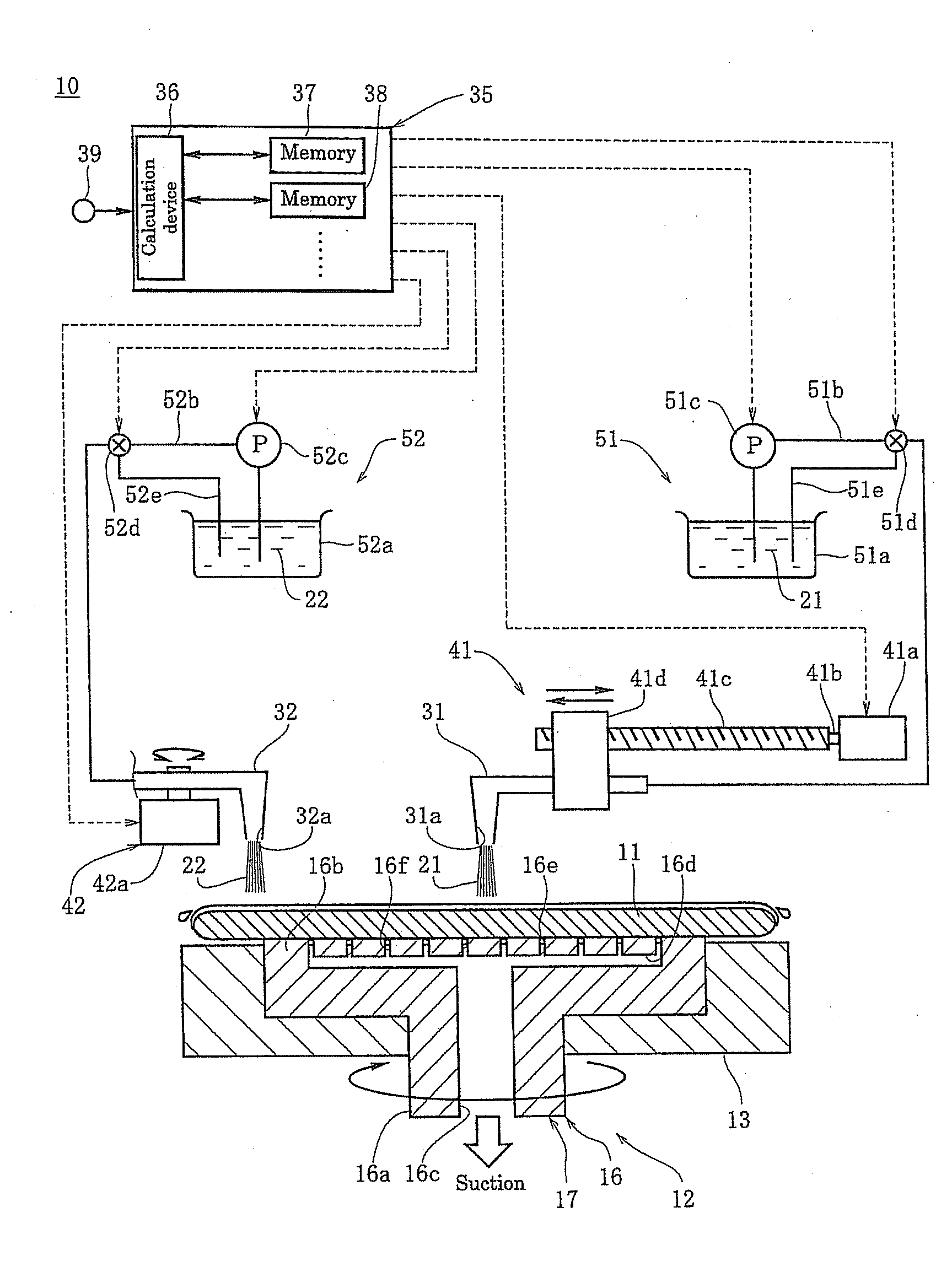
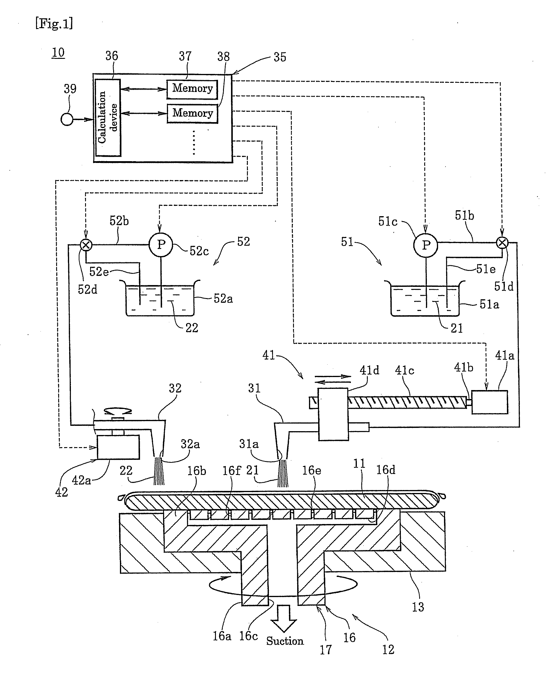
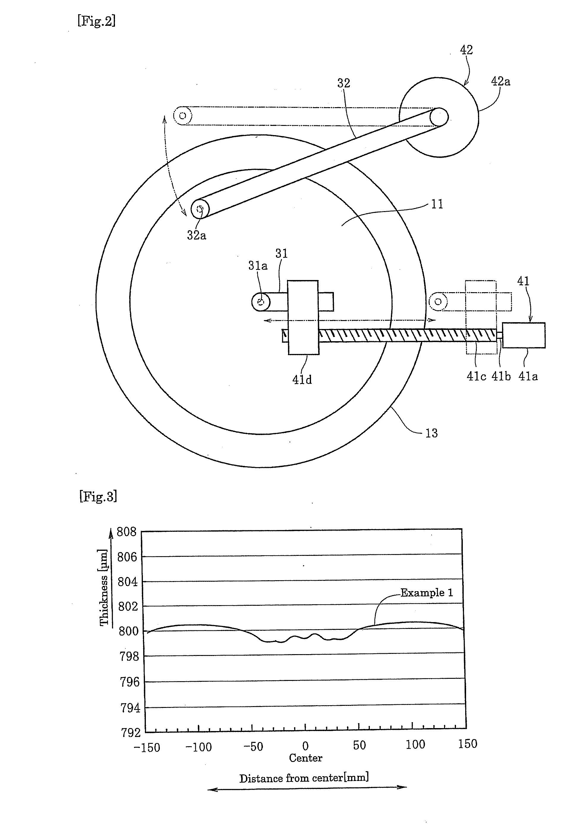
[0045]As shown in FIGS. 1 and 2, a wafer obtained by slicing a silicon single crystal ingot was subjected to chamfering and mechanical grinding (lapping), so that there was also prepared a silicon wafer 11 of 300 mm in diameter of which front and back surfaces were flattened. In addition, a first etching solution 21 was prepared by mixing an aqueous hydrofluoric acid solution at a weight concentration of 50%, an aqueous nitric acid solution at a weight concentration of 70%, and an aqueous phosphoric acid solution at a weight concentration of 85% in a volume ratio of 4:7.4:6 and then reserved in a first tank 51a heated at 30° C. On the other hand, a second etching solution 22 was prepared by mixing 50% by weight concentration of an aqueous fluorine acid solution, 70% by weight concentration of an aqueous nitric acid solution, and 80% by weight concentration of an aqueous phosphoric acid solution in a volume ratio of 4:7.4:6 and then reserved in a second tank 52a heated at 20° C. Unde...

example 2

[0046]Etching of wafer was carried out by the same way as that of Example 1, except that a second etching solution used was an etching solution prepared by mixing an aqueous hydrofluoric acid solution at a weight concentration of 50%, an aqueous nitric acid solution at a weight concentration of 70%, and an aqueous phosphoric acid solution at a weight concentration of 85% at a volume ratio of 3:8:6 and then kept at a temperature of 30° C. Therefore, the etched wafer was provided for Example 2.

example 3

[0047]Etching of wafer was carried out by the same way as that of Example 1, except that the second etching solution was supplied from the second supply nozzle onto the periphery of the front surface of the wafer at a flow rate of 3 l / min. Therefore, the etched wafer was provided for Example 3.


PUM

PropertyMeasurementUnit
temperatureaaaaaaaaaa

Abstract

An object of the present invention is to provide a method for etching a single wafer, which effectively realizes a high flatness of wafer and an increase in productivity thereof. In a method for etching a single wafer, a single thin disk-like wafer sliced from a silicon single crystal ingot is spun, and a front surface of the wafer is etched with an etching solution supplied thereto. In the method, a plurality of supply nozzles are disposed above and opposite to the front surface of the wafer at different portions in the radial direction of the wafer, respectively; and then one or more conditions selected from the group consisting of temperatures, kinds, and supply flow rates of etching solutions from the plurality of supply nozzles are changed.

Description

TECHNICAL FIELD[0001]The present invention relates to a method for etching the front surface of a wafer one by one, where the wafer is rotated while an etching solution is supplied onto the front surface of the wafer.BACKGROUND ART[0002]In general, the process for manufacturing a semiconductor wafer comprises the steps of obtaining wafers by cutting and slicing out of a single crystal ingot, and chamfering the respective wafers, mechanical grinding (lapping), etching, mirror-polishing, and cleaning, thereby producing a wafer with highly precise flatness. The wafer, which has been subjected to the steps for mechanical processing, such as block-cutting, rounding, slicing, and lapping, has a damaged layer (i.e., a processing-strained layer) on the surface thereof. In the process for device production, such a processing-strained layer causes crystal defects, such as slip dislocation, and the mechanical strength of the wafer is then decreased. In addition, it has adverse effects on elect...

Claims


Application Information

Patent Timeline
Patent Type & Authority Applications(United States)
IPC IPC(8): H01L21/306
CPCH01L21/02019H01L21/6708H01L21/30604H01L21/3063
Inventor KOYATA, SAKAEHASHII, TOMOHIROMURAYAMA, KATSUHIKOTAKAISHI, KAZUSHIGEKATOH, TAKEO
Owner SUMCO CORP
Why Eureka
Try Eureka