Imaging apparatus and method for controlling the same

a technology of imaging apparatus and output terminal, which is applied in the field of imaging apparatus, can solve the problems of increasing the cost of the package, the difficulty of mounting constituent parts of the imaging apparatus, and the large number of output terminals of the timing signal generation circuit, so as to reduce the number of terminals, improve transmission characteristics, and reduce nois

Inactive Publication Date: 2009-01-08
CANON KK
View PDF6 Cites 14 Cited by
  • Summary
  • Abstract
  • Description
  • Claims
  • Application Information

AI Technical Summary

Benefits of technology

[0009]Exemplary embodiments of the present invention are directed to an imaging apparatus capable of reducing the number of terminals between an image sensor and a signal generation unit, improving transmission characteristics, and reducing noises generated from the signal generation unit. Furthermore, exemplary embodiments of the present invention are directed to a method for controlling the imaging apparatus.

Problems solved by technology

However, compared to a CCD image sensor, a CMOS image sensor requires a large number of control terminals to enable an imaging apparatus to operate as intended.
Therefore, the conventional method encounters with the difficulty in mounting constituent parts of an imaging apparatus and determining the layout of the parts.
Furthermore, when the number of terminals provided for an image sensor is large, the number of output terminals of the timing signal generation circuit is large.
The cost of the package increases.
Moreover, if numerous wiring lines are provided for transmitting control signals to an image sensor that can operate at a higher speed comparable to the CMOS level, a peripheral analog signal (e.g., output signal of the image sensor) may include a noise component.
A peripheral circuit (e.g., analog processing circuit, analog-to-digital (A / D) converter, etc.) may operate undesirably due to noise.
On the other hand, if the driving ability of a timing signal generation circuit that outputs control signals is decreased, the image sensor may not be driven at a designated speed.
Therefore, the clock signal may generate noises having adverse effects on the image sensor.
Thus, implementing the above-described conventional method is difficult.

Method used


Image

  • Imaging apparatus and method for controlling the same
  • Imaging apparatus and method for controlling the same
  • Imaging apparatus and method for controlling the same

Examples


first exemplary embodiment

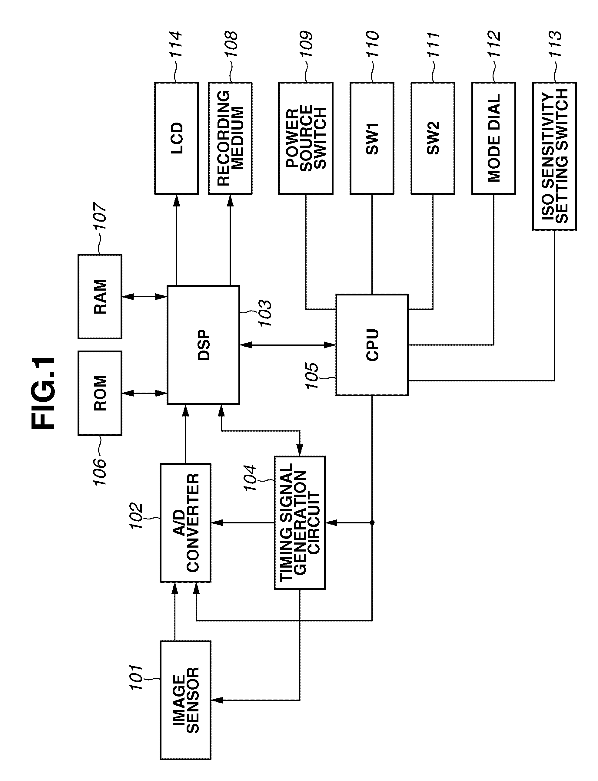
[0027]FIG. 1 is a block diagram illustrating an example configuration of a digital camera, which serves as an imaging apparatus according to a first exemplary embodiment of the present invention.

[0028]The digital camera illustrated in FIG. 1 includes an imaging optical system (not illustrated), an image sensor 101, an analog-to-digital (A / D) converter 102, a digital signal processor (DSP) 103 for image processing, a timing signal generation circuit 104, a central processing unit (CPU) 105, a read-only memory (ROM) 106, a random access memory (RAM) 107, and a recording medium 108. Furthermore, the digital camera includes a power source switch 109, a first shutter switch (SW1) 110, a second shutter switch (SW2) 111, a mode dial 112, an ISO sensitivity setting switch 113, a display unit (LCD) 114, a photometry control unit (not illustrated), and a range-finding control unit (not illustrated).

[0029]When the imaging optical system (not illustrated) forms an optical image of an object in ...

second exemplary embodiment

[0094]A second exemplary embodiment of the present invention differs from the above-described first exemplary embodiment in an internal connection state of a digital camera as illustrated in FIG. 8. Other elements of this exemplary embodiment are similar to those described in the above-described first exemplary embodiment (refer to FIGS. 1 through 3).

[0095]FIG. 8 is a block diagram illustrating an example connection status between the image sensor 101 and the timing signal generation circuit 104 according to an exemplary embodiment.

[0096]As illustrated in FIG. 8, the image sensor 101 and the LVDS receiver 1011 are enclosed in an image sensor package 120. The image sensor 101 includes the S / P conversion block 1012 and the imaging block 1013, which are formed on the same semiconductor chip. The LVDS receiver 1011 is formed on another semiconductor chip. The timing signal generation circuit 104 includes the timing generator unit 1041, the P / S conversion block 1042, the LVDS driver 1043...

third exemplary embodiment

[0106]A third exemplary embodiment of the present invention provides a digital camera illustrated in FIG. 10, which is different from the digital camera according to the above-described first exemplary embodiment. Other elements of this exemplary embodiment are similar to those described in the above-described first exemplary embodiment (refer to FIGS. 2 and 3).

[0107]FIG. 10 is a block diagram illustrating an example configuration of a digital camera, which serves as an imaging apparatus according to the third exemplary embodiment.

[0108]In FIG. 10, the digital camera includes the image sensor 101, the A / D converter 102, the DSP 140, the CPU 105, the ROM 106, the RAM 107, and the recording medium 108. The DSP 140 includes the timing signal generation circuit 104. Furthermore, the digital camera includes the power source switch 109, the first shutter switch (SW1) 110, the second shutter switch (SW2) 111, the mode dial 112, the ISO sensitivity setting switch 113, and the display unit (...


PUM


Abstract

In an imaging apparatus, a first conversion unit multiplexes input signals including control signals for driving an image sensor to generate a multiplex signal having a frequency higher than those of the input signals. A transfer unit transfers the multiplexed signal generated by the first conversion unit according to low-voltage differential signaling. A reception unit receives the multiplexed signal from the transfer unit. A second conversion unit extracts the control signals for driving the image sensor from the multiplexed signal received by the reception unit. A third conversion unit performs at least one of correction processing and development processing on a signal generated by the image sensor. A signal generation unit generates and supplies processing timing control signals to the first conversion unit and the third conversion unit.

Description

BACKGROUND OF THE INVENTION[0001]1. Field of the Invention[0002]The present invention relates to an imaging apparatus including an image sensor that generates an image signal of a captured object and a timing signal generation circuit that drives the image sensor. Furthermore, the present invention relates to a method for controlling the imaging apparatus.[0003]2. Description of the Related Art[0004]In general, charge-coupled device (CCD) image sensors and complementary metal-oxide semiconductor (CMOS) image sensors are installed on various imaging apparatuses including digital cameras and digital video cameras. An imaging apparatus equipped with an image sensor includes a timing signal generation circuit that supplies a timing signal (control signal) to the image sensor. The timing signal generation circuit has important roles. As discussed in Japanese Patent Application Laid-Open No. 2002-64753, there is a conventional method for reducing the number of input terminals provided for...

Claims


Application Information

Patent Timeline
Patent Type & Authority Applications(United States)
IPC IPC(8): H04N5/335H04N5/228H04N5/357H04N5/374H04N5/376
CPCH04N5/335H04N5/3765H04N5/3577H04N25/617H04N25/00H04N25/745
Inventor KITANI, KAZUNARI
Owner CANON KK
Why Eureka
Try Eureka