Avalanche Photodiode With Edge Breakdown Suppression

a photodiode and edge technology, applied in the field ofavalanche photodiodes, can solve the problems of poor gain uniformity and premature breakdown, small design window, and large noise performance and bandwidth of apd, and achieve the effect of preventing the introduction of new dopants, enhancing gain uniformity, and reducing nois

Active Publication Date: 2009-01-22
LUMENTUM OPERATIONS LLC
View PDF12 Cites 14 Cited by
  • Summary
  • Abstract
  • Description
  • Claims
  • Application Information

AI Technical Summary

Benefits of technology

[0011]The present invention has found that an avalanche photodiode can provide enhanced gain uniformity by tailoring the diffused p-n junction profile. The tailoring is achieved by a two stage doping process incorporating a solid source diffusion in combination with conventional gas source diffusion. The solid source diffusion material is selected such that the solubility of the dopant is higher in the solid source diffusion material compared to the multiplication layer material. The solid source material is patterned so that is has a finite lateral extent. Prior to a first diffusion step, a window is created that exposes the multiplication layer material and the solid source material. As shown in FIG. 2, during the first diffusion, a dopant containing gas impinges on the window, diffusing dopant into the multiplication layer directly in region I, and in region II diffusing dopant into the multiplication layer material after first diffusing through the solid source material. Prior to the second diffusion, a new window is opened exclusively in the central portion of the solid source material, thus preventing further introduction of new dopant in region I and preventing further introduction of new dopant in a portion of region II (labeled as IIA). Thus, there are three distinct diffusion regions during the second diffusion. Region I comprises a finite source diffusion with relatively low dopant concentration (limited by the solubility of the dopant in the multiplication layer). Region IIA comprises a finite source diffusion from the solid source material with a relatively higher dopant concentration (limited by the solubility of the dopant in the solid source material). Region IIB comprises an infinite diffusion source from the solid source material as it is continually charged with new dopant from the external gas source. The result is that both the dopant concentration and the diffusion depth decrease gradually from the center to the edge of the device. This tailored diffusion profile enables control of the electric field distribution such that edge breakdown is suppressed.
[0012]The solid source also comprises a material which is lattice matched or at least compatible with the crystal structure growth for epitaxial growth on the multiplication layer. The solid diffusion source can additionally serve as a contact layer for the completed device. In a preferred embodiment, a thin InGaAs slab of finite lateral extent is selected as a finite solid source for the second diffusion into the InP multiplication layer to smooth the transition between the first and second diffusion profile.

Problems solved by technology

These increased edge fields lead to larger gain at the edge of the active region which causes a poor gain uniformity and premature breakdown, typically referred to as “edge breakdown”.
The poor gain uniformity has markedly deleterious effects on device performance, particularly the noise performance and bandwidth of the APD.
However, in reality, the design window is quite small.
And if the step is too big, it will not provide enough help to smooth out the second diffusion corner, resulting in electrical field E2 larger than Ec.
However, in use the etch depth and sidewall curvature is very difficult to control by wet chemical etching.
But dry etching damages the InP surface severely and the surface condition / reconstruction is critical to achieve a repeatable diffusion profile.

Method used


Image

  • Avalanche Photodiode With Edge Breakdown Suppression
  • Avalanche Photodiode With Edge Breakdown Suppression
  • Avalanche Photodiode With Edge Breakdown Suppression

Examples


Embodiment Construction

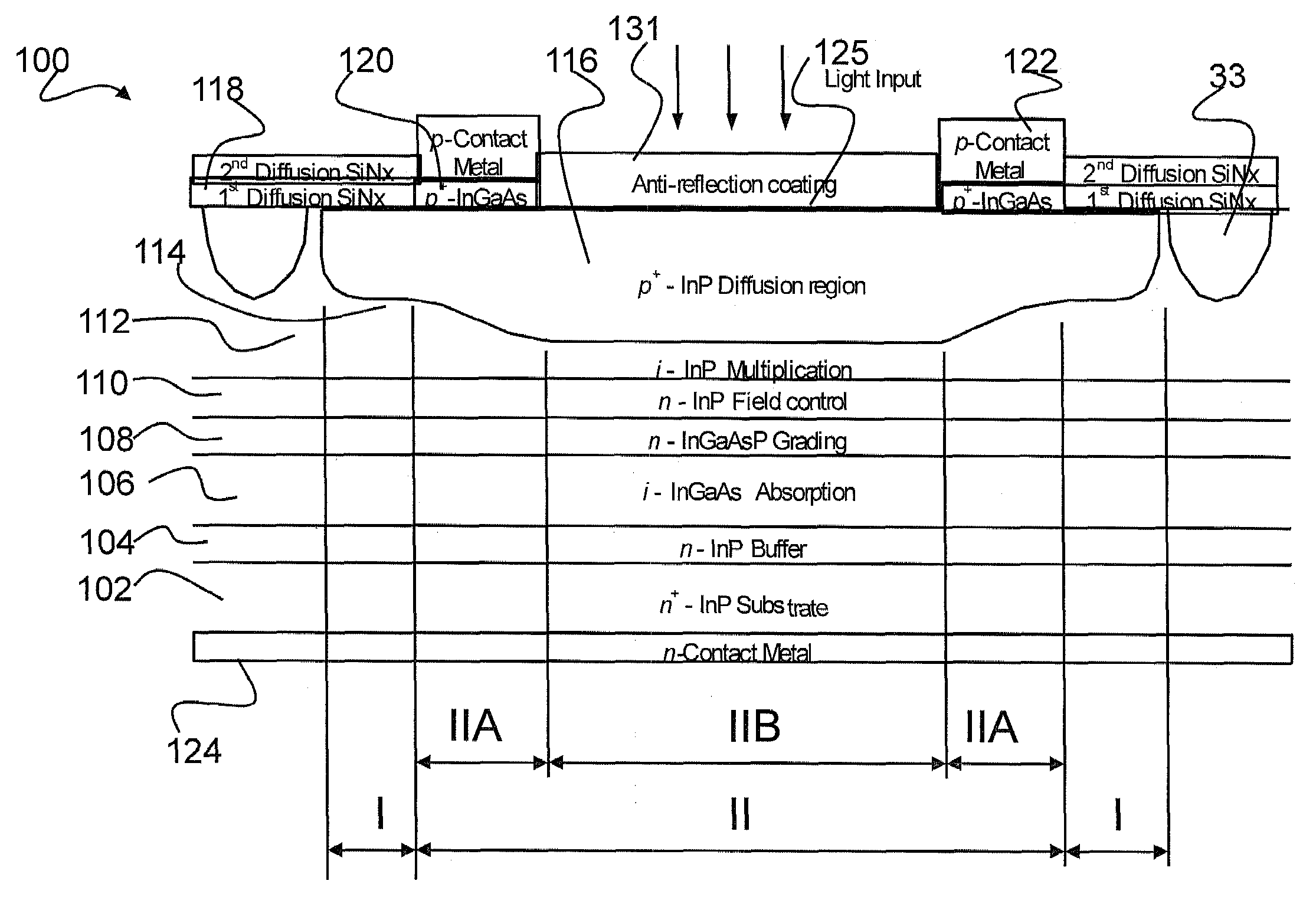
[0046]The present invention provides an SAM-APD having an avalanche multiplication structure to suppress edge breakdown. The schematic structure is shown in FIG. 2. The APD 100 has a separate absorption and multiplication (SAM) structure. The SAM structure is grown on n-doped InP substrate 102. A typical SAM layer structure consists of an n-doped InP buffer layer 104 (0.3-1 μm), an unintentionally doped InGaAs absorption layer 106 (0.4-2 μm), a GaInAsP grading layer 108 (0.05-0.2 μm), an n-doped InP field control layer 110 and an unintentionally doped InP multiplication layer 112. The multiplication layer 112 includes the p-n junction 114 at the diffusion profile formed by Zn diffusion. A thin InGaAs layer slab 120 is grown on InP multiplication layer 112. The thickness of this InGaAs slab layer 120 is in the range of 0.05-0.5 μm. It can be unintentionally doped or heavily doped with p-type dopant such as Zn. The multiplication layer 112, active region 116 and guard rings 33 are enc...


PUM


Abstract

The invention relates to an avalanche photodiode having enhanced gain uniformity enabled by a tailored diffused p-n junction profile. The tailoring is achieved by a two stage doping process incorporating a solid source diffusion in combination with conventional gas source diffusion. The solid source diffusion material is selected for its solubility to the dopant compared to the solubility of the multiplication layer to dopant. The solid source has a diameter between the first and second diffusion windows. Thus, there are three distinct diffusion regions during the second diffusion. The dopant in the multiplication layer at the edge region, the dopant from the solid source material with a relatively higher dopant concentration (limited by the solubility of the dopant in the solid source material) at the intermediate region, and the central region exposed to an infinite diffusion source from the solid source material as it is continually charged with new dopant from the external gas source. The result is that both the dopant concentration and the diffusion depth decrease gradually from the center to the edge of the device. This tailored diffusion profile enables control of the electric field distribution such that edge breakdown is suppressed.

Description

CROSS-REFERENCE TO RELATED APPLICATIONS[0001]This application claims priority from U.S. Provisional Application No. 60 / 950,403 filed Jul. 18, 2007 herein incorporated by reference.TECHNICAL FIELD[0002]The present application relates to an avalanche photodiode (APD) having an avalanche multiplication structure to suppress edge breakdown. The present invention further relates to a method of making an avalanche multiplication structure in an avalanche photodiode with edge breakdown suppression.BACKGROUND OF THE INVENTION[0003]Avalanche photodiode structures that have separate absorption and multiplication layers (SAM-APDs) can provide electrical output signals with high fidelity (i.e. low noise). For use in telecommunications applications, the APD is electrically biased such that the electrical response is substantially linear with optical power. Although the APD requires higher operating voltages, the internal gain of the APD provides a significant increase in receiver sensitivity com...

Claims


Application Information

Patent Timeline
Patent Type & Authority Applications(United States)
IPC IPC(8): H01L31/0336H01L31/18
CPCH01L21/2258H01L31/1035Y02E10/544H01L31/184H01L31/1075
Inventor PAN, ZHONGVENABLES, DAVIDCIESLA, CRAIG
Owner LUMENTUM OPERATIONS LLC
Why Eureka
Try Eureka