

Method for manufacturing SOI wafer
a manufacturing method and technology of soi wafers, applied in semiconductor/solid-state device manufacturing, basic electric elements, electric apparatus, etc., can solve the problems of difficult constant balance in a radial direction of various factors, difficulty in polishing or polishing pads in fixed state, etc., and achieve excellent productivity and superior film thickness uniformity
- Summary
- Abstract
- Description
- Claims
- Application Information
AI Technical Summary
Benefits of technology
Problems solved by technology
Method used
Image

Examples
example
[0092]The method for manufacturing an SOI wafer according to the present invention will now be further specifically explained based on examples and comparative examples.
examples 7 to 12
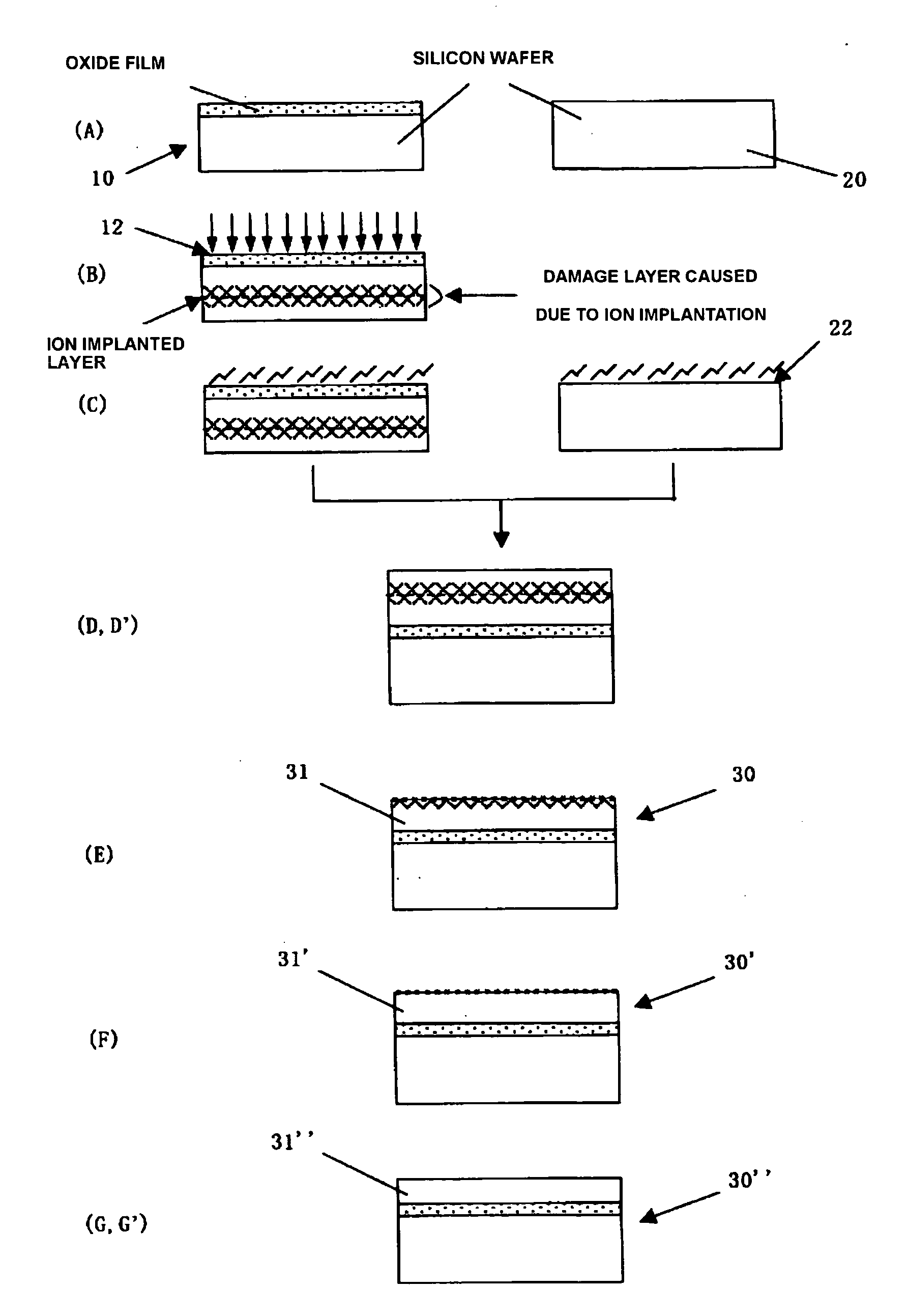
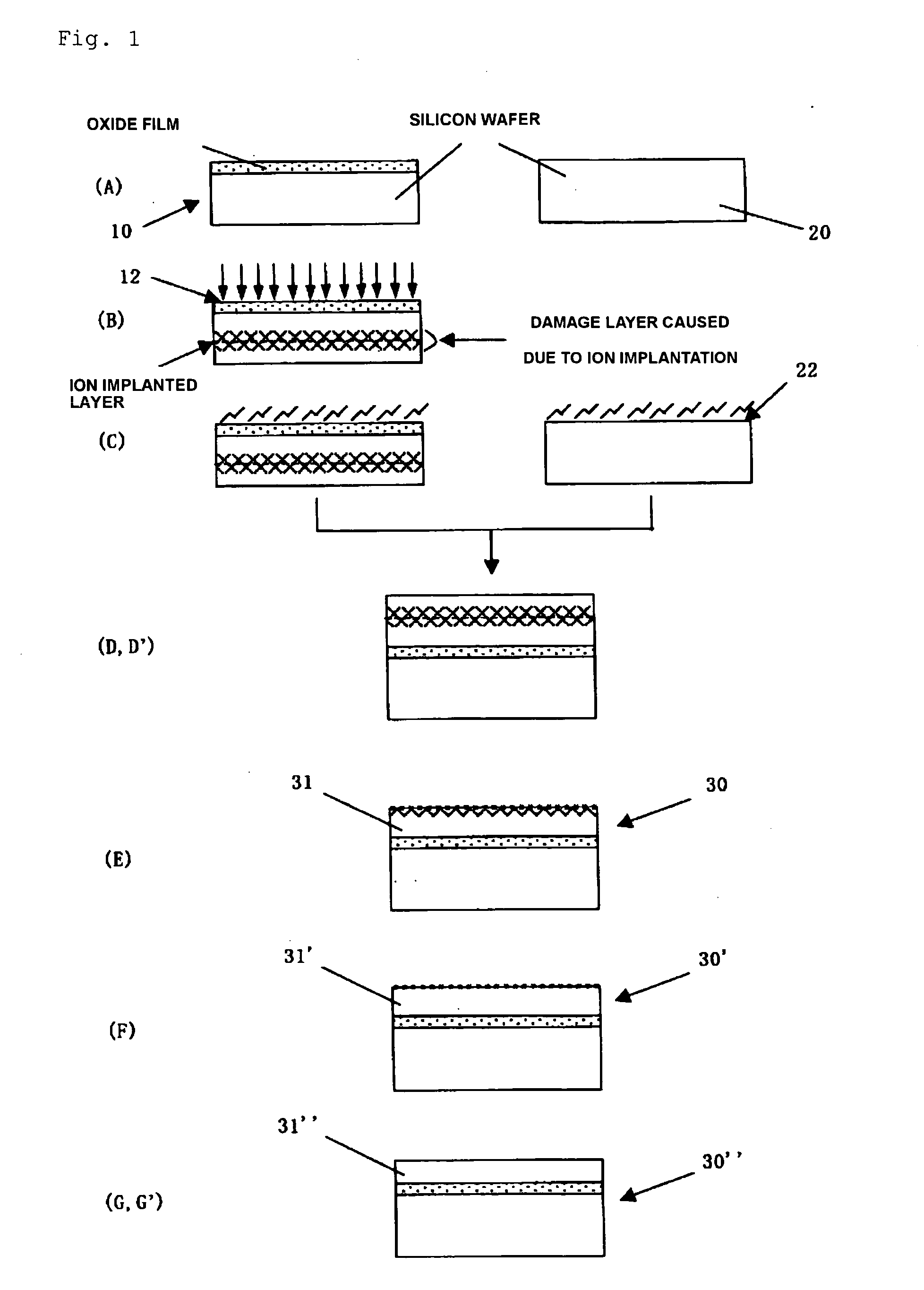
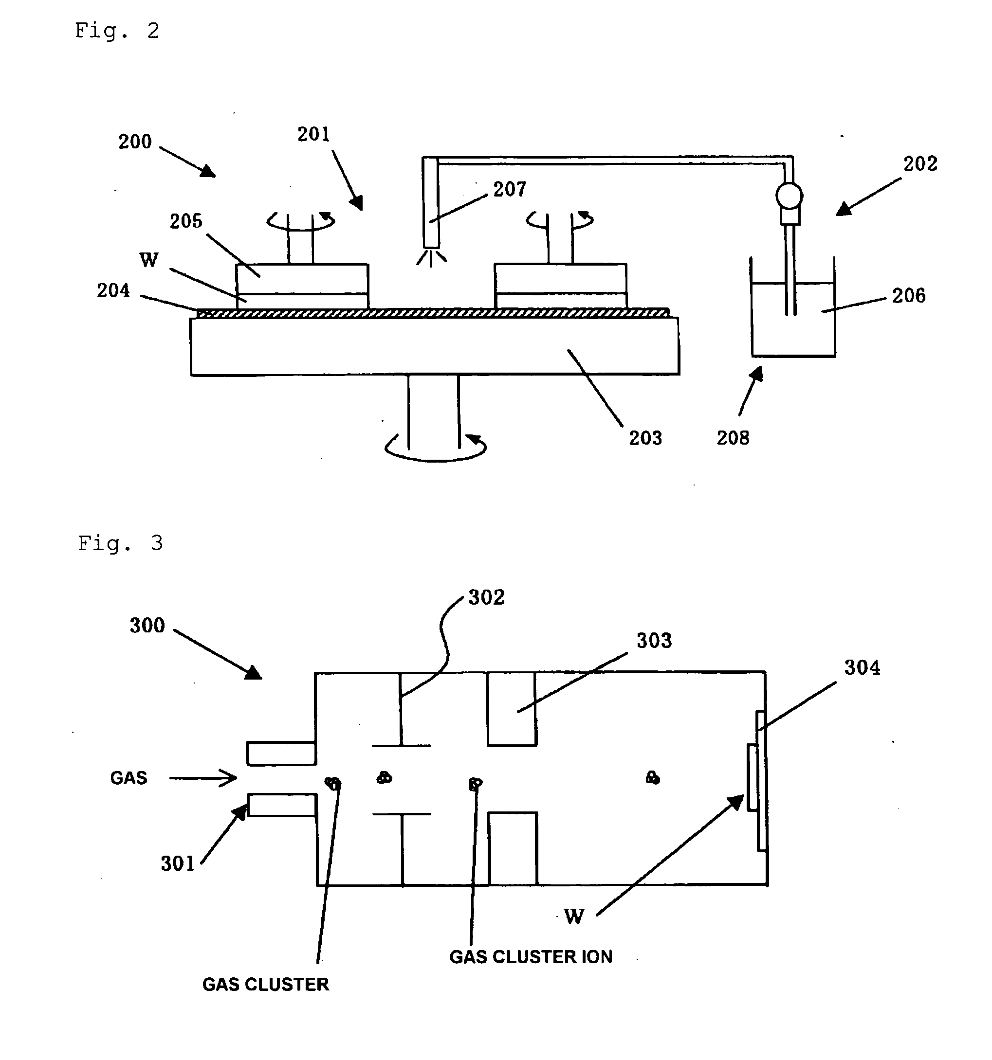
[0123]An SOI wafer was manufactured like Examples 1 to 6 except that a surface of an SOI layer was etched for 10 to 50 nm based on a GCIB processing in place of chemical mechanical polishing after a heat treatment following delamination.
[0124]SF6 was used as a raw material gas, a cluster size was 1000 atoms or above, a current applied to an ionizing electrode was 300 μA, and a voltage applied to an accelerating electrode was 30 kV.
[0125]Examining the SOI layer of the thus obtained SOI wafer, it was revealed that the high-quality SOI layer having a mirror-finished surface and a uniform film thickness was obtained like Examples 1 to 6.
[0126]It is to be noted that the present invention is not restricted to the foregoing examples. The examples are just exemplifications, and any examples which have the same structure and demonstrate the same functions and effects as those in the technical concept explained in claims of the present invention are included in the technical scope of the pres...
PUM
 Abstract
Description
Claims
Application Information