Semiconductor device

Active Publication Date: 2009-01-29
RENESAS ELECTRONICS CORP
View PDF15 Cites 58 Cited by
  • Summary
  • Abstract
  • Description
  • Claims
  • Application Information

AI Technical Summary

Benefits of technology

[0010]The present invention is made in view of the above problems, an object thereof is to

Problems solved by technology

On the other hand, an increase in consumption current involved in such achievement of high speeds makes an increasing problem of causing characteristic degradation due to power supply noise such as IR-Drop (i.e., assuming that when current I flows through a path and the resistance value of the path is R, a potential difference represented as I×R is generated at both ends of the path).
With this method, there has been a tendency that the number of interconnects of connecting transistors and the number of interconnects of connecting transistors and power supply lines are increased to make the interconnect layout complicated.
How

Method used


Image

  • Semiconductor device
  • Semiconductor device
  • Semiconductor device

Examples


Example

First Embodiment

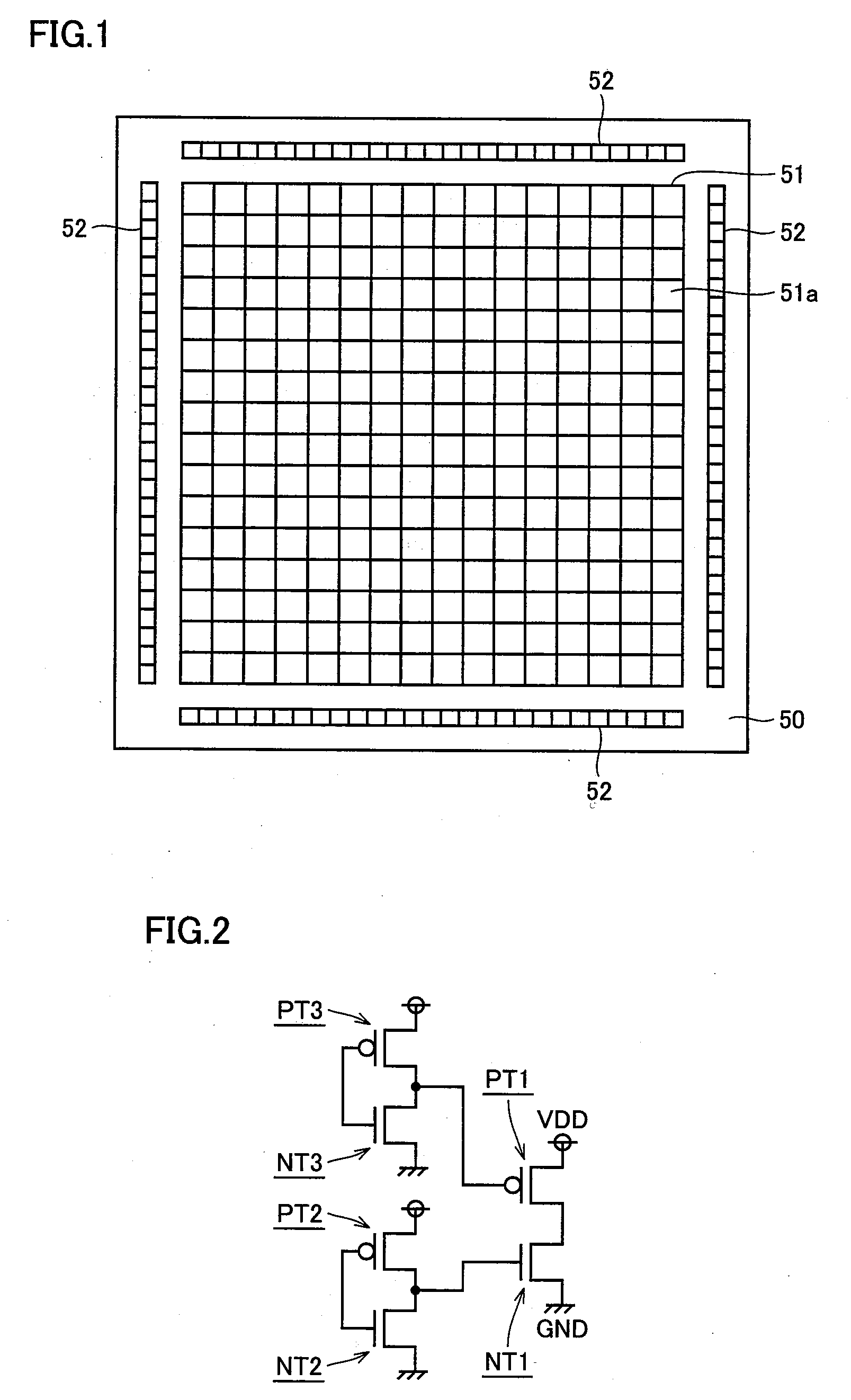
[0042]With reference to FIG. 1, a semiconductor device (e.g., a semiconductor chip) 50 mainly includes on the surface of semiconductor device 50 a standard cell region 51, input / output (I / O) cell regions 52 arranged around standard cell region 51, and pads (not shown) for use in input and output to and from the outside.

[0043]Standard cell region 51 has a plurality of standard cells 51a arranged in a matrix. In an SOC using a standard cell library, formed in this standard cell region 51 are a central processing unit (CPU), a random access memory (RAM), a first-in first-out (FIFO), a small computer system interface (SCSI), a sea of gate (SOG), etc.

[0044]With reference to FIG. 2, a circuit of a function element formed in standard cell 51a is, e.g., a partial circuit of a buffer for tri state, and has an output stage and a driver. The output stage is made, e.g., of a CMOS inverter including a pMOS transistor PT1 and an nMOS transistor NT1. The driver is composed, e.g., ...

Example

Second Embodiment

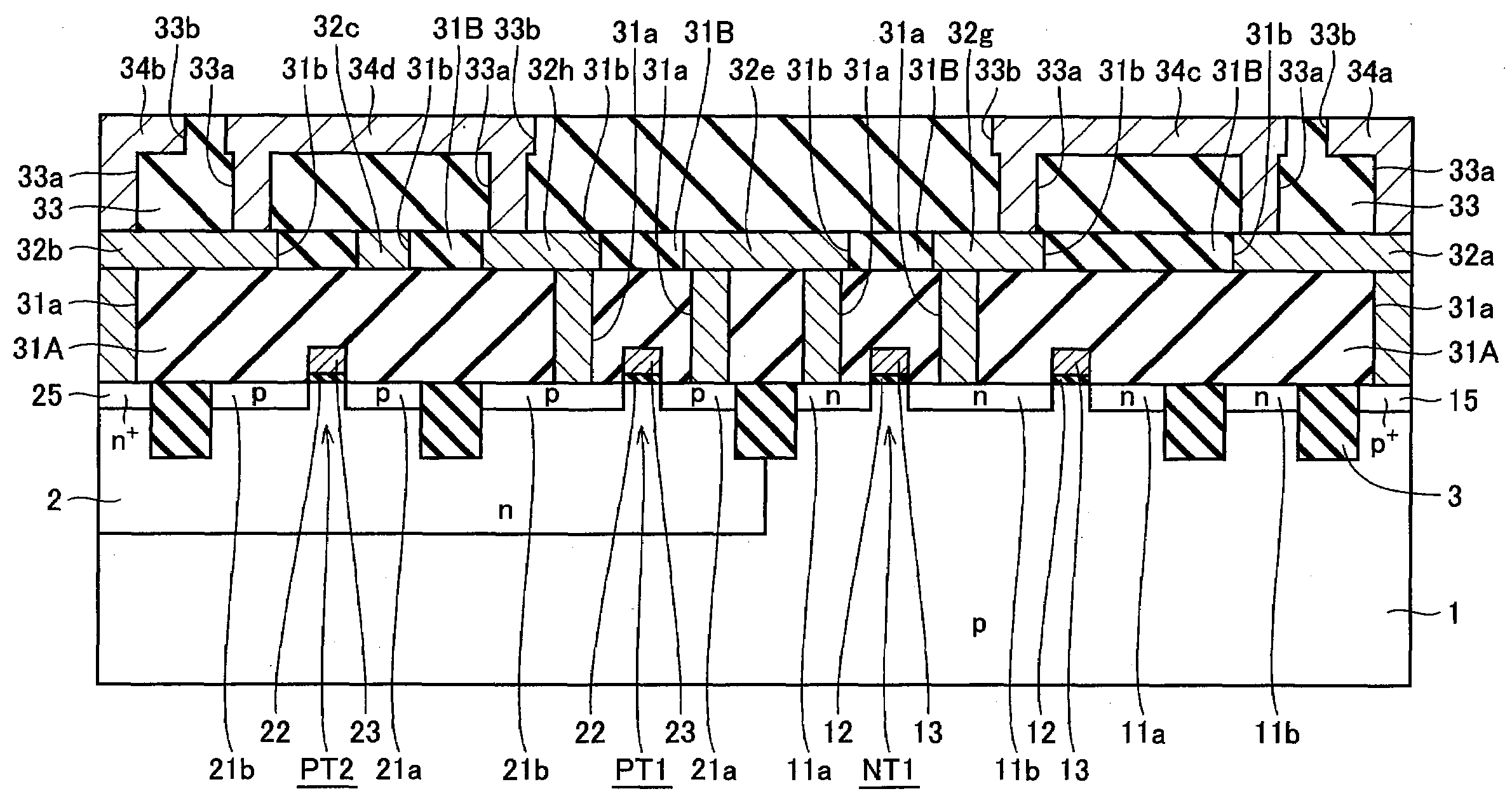
[0084]With reference to FIGS. 5 and 6, in the present embodiment, a configuration will be described in which a CMOS inverter including nMOS transistor NT1 and pMOS transistor PT1 is formed in each of a plurality of standard cells 51a.

[0085]P-type well region 1 is formed on the surface of a semiconductor substrate and n-type well region 2 is selectively formed on the surface in p-type well region 1. Formed on the surface in p-type well region 1 is nMOS transistor NT1. Formed on the surface in n-type well region 2 is pMOS transistor PT1.

[0086]In such a manner as to extend in the lateral direction (X direction in FIG. 5) along one (boundary on the lower side in the Y direction in FIG. 5) of the boundaries in the vertical direction (Y direction in FIG. 5) of standard cell 51a, p+ region 15 is formed on the surface in p-type well region 1. In such a manner as to extend in the lateral direction (X direction in FIG. 5) along the other (boundary on the upper side in the Y...

Example

Third Embodiment

[0121]The present embodiment realizes the circuit configuration shown in FIG. 2 by modifying the configuration of the second embodiment.

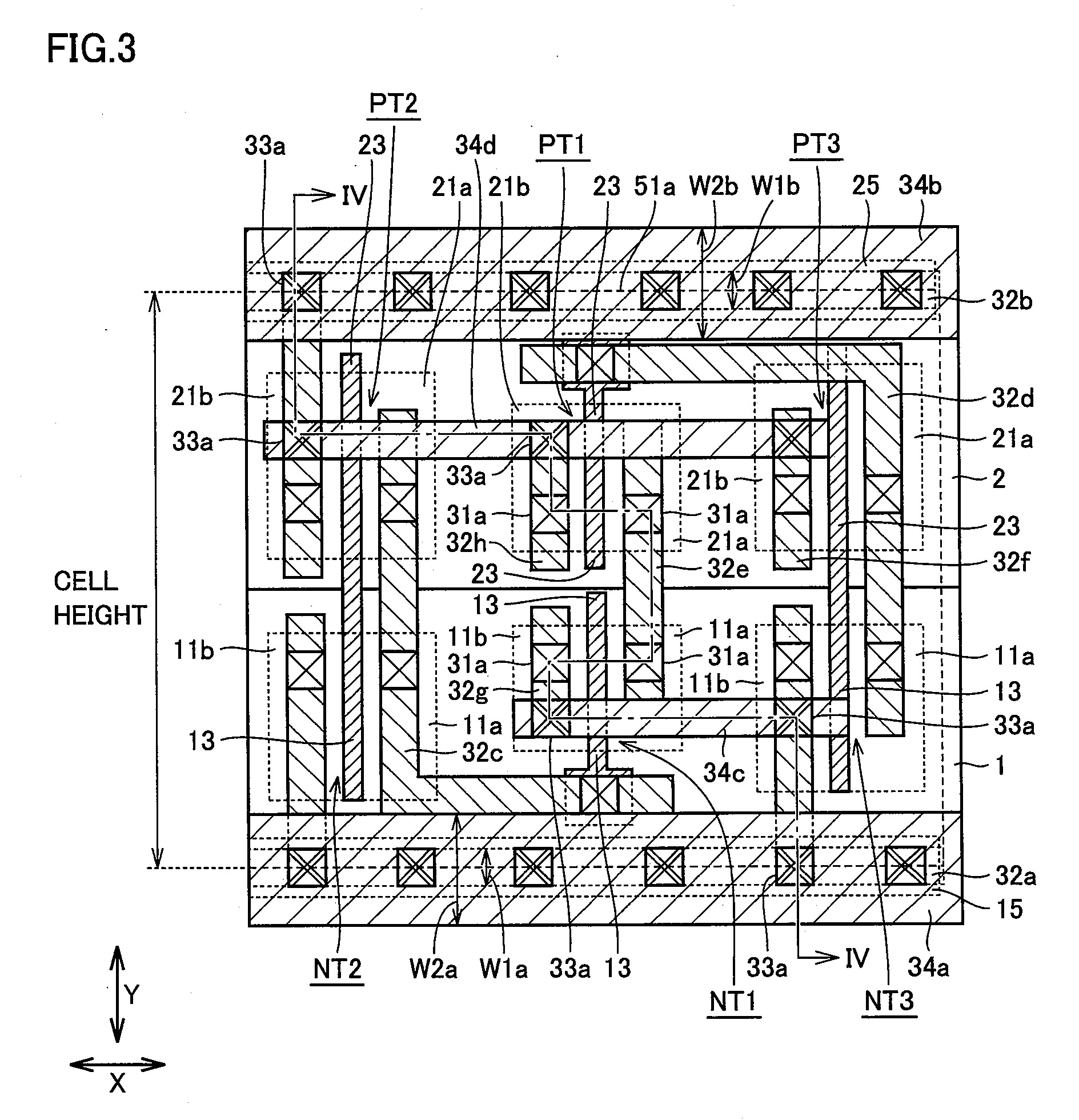
[0122]With reference to FIGS. 9 and 10, in the configuration of the embodiment, for example, nMOS transistor NT1 and pMOS transistor PT1 in the central standard cell 51a, among three aligned standard cells 51a having inverters, correspond to the CMOS inverter of the output stage in FIG. 2.

[0123]A CMOS inverter including nMOS transistor NT2 and pMOS transistor PT2 in right-hand standard cell 51a adjacent to the central standard cell 51a in the drawing and a CMOS inverter including nMOS transistor NT3 and pMOS transistor PT3 of left-hand standard cell 51a adjacent to the central standard cell 51a in the drawing correspond to the driver in FIG. 2.

[0124]Gate electrode layer 13 of nMOS transistor NT1 and gate electrode layer 23 of pMOS transistor PT1 in the central standard cell 51a are electrically separated. An interconnect layer 32e1 ...


PUM


Abstract

CMOS inverters are included in a standard cell. Power supply lines are electrically connected to CMOS inverters, and include lower layer interconnects and upper layer interconnect. Lower layer interconnects extend along a boundary of standard cells adjacent to each other and on the boundary. Upper layer interconnects are positioned more inside in standard cell than lower layer interconnects, as viewed from a plane. CMOS inverters are electrically connected through upper layer interconnects to lower layer interconnects. Thus, a semiconductor device is obtained that can achieve both higher speeds and higher integration.

Description

BACKGROUND OF THE INVENTION[0001]1. Field of the Invention[0002]The present invention relates to semiconductor devices, and particularly to semiconductor devices having a plurality of aligned standard cells.[0003]2. Description of the Background Art[0004]In recent years, layout design using a standard cell library is generally performed in system on chip (SOC) because of increasing scale of circuit integration. As the advanced functions and performances of SOC are achieved, the demand for higher integration and higher speeds of the standard cell library increases. On the other hand, an increase in consumption current involved in such achievement of high speeds makes an increasing problem of causing characteristic degradation due to power supply noise such as IR-Drop (i.e., assuming that when current I flows through a path and the resistance value of the path is R, a potential difference represented as I×R is generated at both ends of the path).[0005]Conventionally, there is a config...

Claims


Application Information

Patent Timeline
IPC IPC(8): H01L27/10
CPCH01L27/0207
Inventor TSUDA, NOBUHIRO
Owner RENESAS ELECTRONICS CORP
Why Eureka
Try Eureka