

Tunnel Field-Effect Transistor with Narrow Band-Gap Channel and Strong Gate Coupling
a field-effect transistor and tunnel-effect technology, applied in semiconductor devices, diodes, electrical devices, etc., can solve the problems of inability to achieve fast switching at low operation voltage for future nanometer devices, inability to achieve fast switching at low operation voltage, and inability to achieve ultra thin body mosfet on soi or finfet to achieve close to, but not below, the limit of 60 mv/decade, etc., to achieve the effect of reducing leakage curren
- Summary
- Abstract
- Description
- Claims
- Application Information
AI Technical Summary
Benefits of technology
Problems solved by technology
Method used
Image

Examples
first embodiment
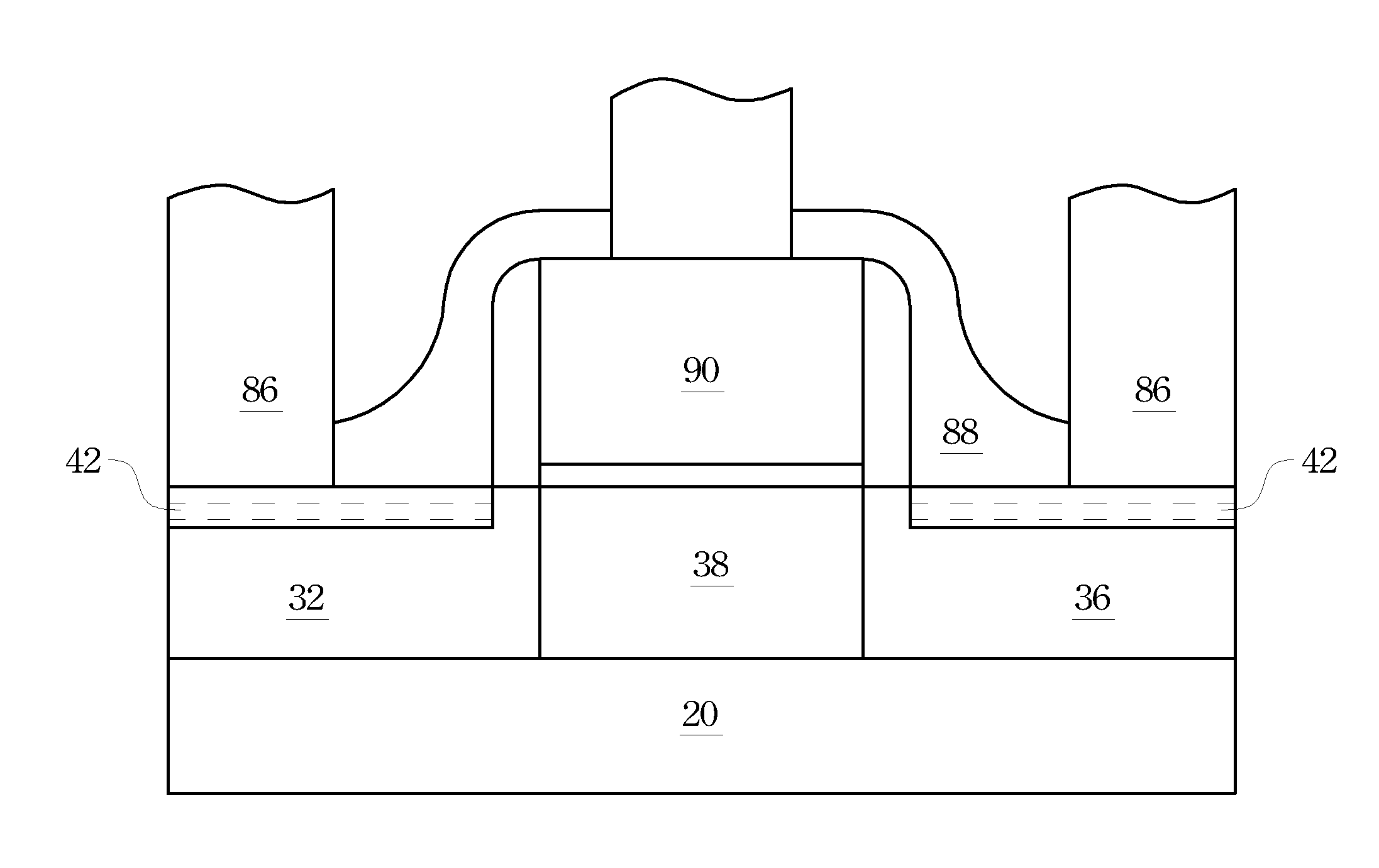
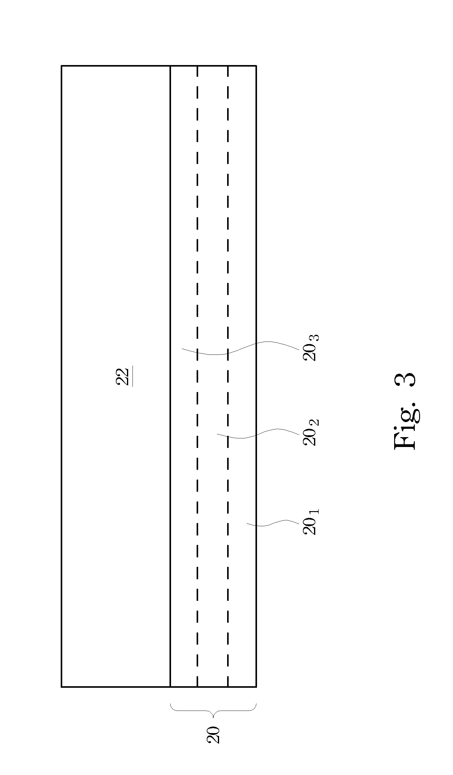
[0030]the present invention is provided in FIGS. 3 through 10. Referring to FIG. 3, substrate 20 is provided. In an embodiment, substrate 20 is a bulk substrate comprising a single crystalline semiconductor material, such as silicon, or a compound semiconductor material. In other embodiments, substrate 20 may include more than one semiconductor layer. For example, substrate 20 may have a silicon-on-insulator or silicon-on-carbide structure, including silicon layer 203 on insulator layer 202. Insulator layer 202 may further be located on semiconductor layer 201. In yet other embodiments, substrate 20 includes an insulator.
[0031]Low (energy) band-gap layer 22 is formed over substrate 20. Throughout the description, the term “low band-gap” refers to band-gaps lower than the band-gap of silicon (1.12 eV). In the preferred embodiment, low band-gap layer 22 is formed of silicon germanium (SiGe). In other embodiments, other semiconductor materials having low band-gaps, such as Ge, GaAs, In...
PUM
 Abstract
Description
Claims
Application Information