Sensing devices from molecular electronic devices utilizing hexabenzocoronenes

a technology of electronic devices and sensing devices, applied in nanoinformatics, instruments, coatings, etc., can solve the problems of difficult bonding between organic molecules and metal electrodes, difficult bridging, and great challenges in selecting appropriate molecules

Inactive Publication Date: 2009-01-29
THE TRUSTEES OF COLUMBIA UNIV IN THE CITY OF NEW YORK
View PDF1 Cites 28 Cited by
  • Summary
  • Abstract
  • Description
  • Claims
  • Application Information

AI Technical Summary

Benefits of technology

[0013]The present invention provides techniques for precisely and / or functionally cutting single SWNTs, and selecting and / or synthesizing appropriate molecules as molecular wires to bridge the gap formed in the cut SWNTs.

Problems solved by technology

However, the selection of appropriate molecules has proven to be a great challenge.
However, due to the constraints of traditional lithography, the gaps between the metal electrodes are usually large compared to the size of small organic molecules, making the bridging very difficult.
However, bonding between organic molecules and metal electrodes is difficult to accomplish, and is notoriously ill-defined even when accomplished.
1668 (2005), even if more conductive contact chemistry is used, such as carbenes on transition metals and on metal carbides, molecular-scale metal electrodes are extremely difficult to fabricate and lack specific chemistry for molecular attachment at their ends.
This ill-defined bonding may result in unpredictable transport properties of electrons through the devices.
However, this benefit can also be a barrier for new generation nanometer-scale transistors.
Reducing the width of active channels in these transistors is still a great challenge.
However, since SWNTs have a large surface area and multitude of potential reaction centers, the specificity and sensitivity of the detection are still limited.

Method used


Image

  • Sensing devices from molecular electronic devices utilizing hexabenzocoronenes
  • Sensing devices from molecular electronic devices utilizing hexabenzocoronenes
  • Sensing devices from molecular electronic devices utilizing hexabenzocoronenes

Examples


example 1

Preparation of Contorted Hexabenzocoronenes

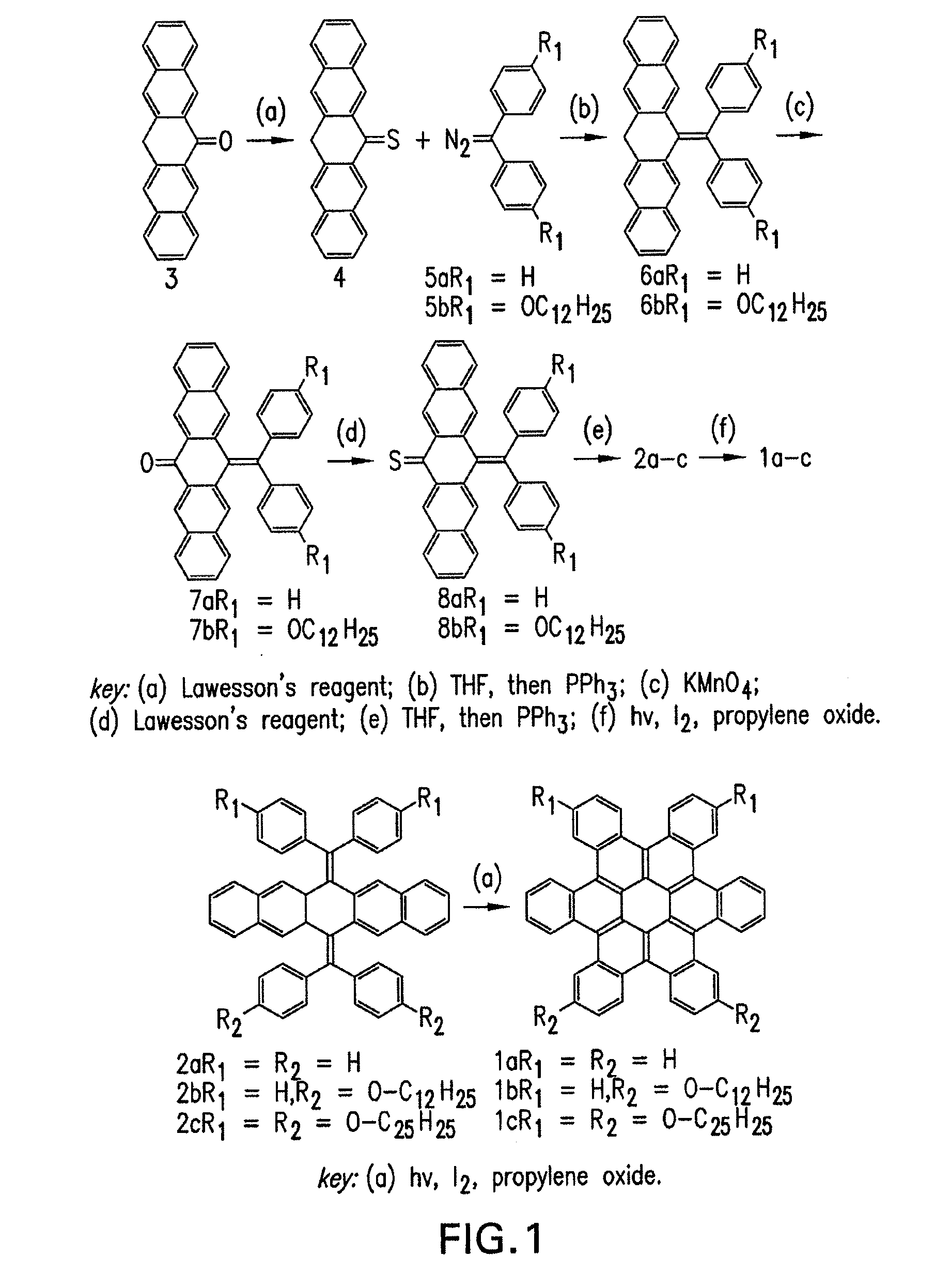
[0084]The syntheses for preparing contorted hexabenzocoronenes of formula 1 are schematically shown in FIG. 1. Ketone 3 was synthesized according to the well-known procedure disclosed in E. Clar,Chemische Berichte vol. 82, p. 495 (1949), the contents of which are incorporated by reference herein.

[0085]Synthesis of thioketone 4. Ketone 3 (4.4 g, 14.9 mmol) and Lawesson's reagent (0.7 eq, 4.2 g, 10.4 mmol) were added to 500 mL of toluene. The solution was heated to 80° C. for 2 hours. The dark green solution was allowed to cool to room temperature and 1200 mL of a 4:1 v / v mixture of hexanes and CH2Cl2 was added. Filtration through a plug of silica gel and a small amount of the same mixture of hexanes and CH2Cl2 was used to wash the remaining product from the silica gel. 3 was isolated as a green solid (2.2 g, 47%) after removal of the solvent and triturating with cold hexanes.

[0086]Synthesis of diphenyldiazomethane 5a: A mixture of 4,4′-dihyd...

example 2

Preparation of a Transistor Device Based on Contorted HBCs

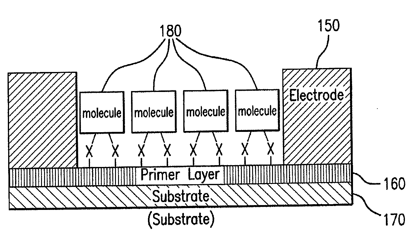
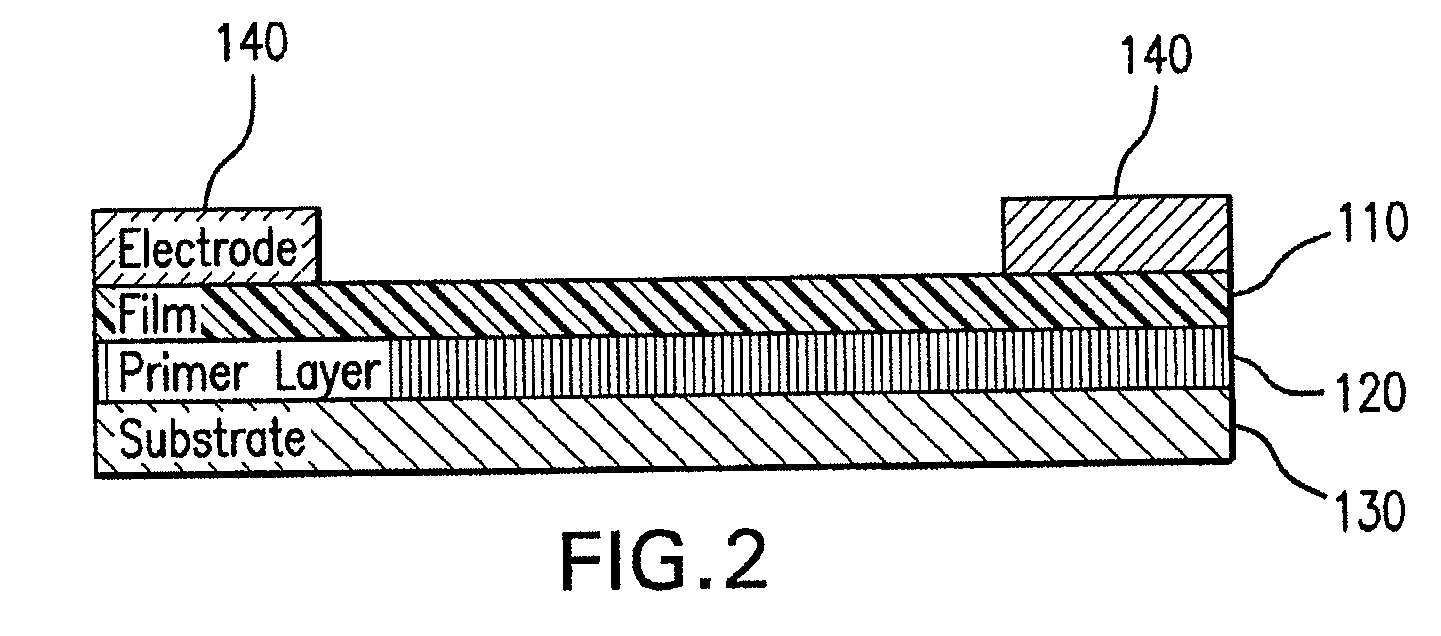
[0100]Compounds of the formula 1c were spin-cast from 1,2-dichloroethane or CHCl3 to form uniform films (approximately 100-nm thick) on top of a SiO2 substrate, and then Au was deposited as source and drain electrodes by thermal evaporation onto the spin-cast films through a metal-shadow mask. A transistor device thus obtained is illustrated schematically in FIG. 2. The transconductance and transistor output are shown in FIGS. 10A and 10B.

[0101]The mobility (0.02 cm2 V−1 s−1) shown in FIG. 10B is calculated from the linear portion of the data in FIG. 10B, and was based on a capacitance of 11.3 nF cm−2 for the gate dielectric layer of 300 nm of SiO2 and a monolayer of octadecyltrichlorosilane, obtained from a series of measurements over a range of frequencies. Other critical parameters, such as the threshold voltage for the device to turn on (as low as −3 V) and the on / off current ratios in the device (106:1), are also very go...

example 3

Fabrication of a Cut SWNT-Film Transistor Device

[0106]A compound of the formula 1c was spin cast onto the gap between a cut SWNT such that it covered gap of the cut SWNT but did not span the metal electrodes (shown in FIG. 15A). The device obtained shows p-type hole transporting semiconductor behavior (see FIG. 15B), but requires greater gate bias than a monolayer device where R2 is COCl is used where surface attachment is effected.


PUM

PropertyMeasurementUnit
diametersaaaaaaaaaa
RF poweraaaaaaaaaa
temperatureaaaaaaaaaa

Abstract

The present invention generally relates to the fabrication of molecular electronics devices from molecular wires and Single Wall Nanotubes (SWNT). In one embodiment, the cutting of a SWNT is achieved by opening a window of small width by lithography patterning of a protective layer on top of the SWNT, followed by applying an oxygen plasma to the exposed SWNT portion. In another embodiment, the gap of a cut SWNT is reconnected by one or more difunctional molecules having appropriate lengths reacting to the functional groups on the cut SWNT ends to form covalent bonds. In another embodiment, the gap of a cut SWNT gap is filled with a self-assembled monolayer from derivatives of novel contorted hexabenzocoranenes. In yet another embodiment, a device based on molecular wire reconnecting a cut SWNT is used as a sensor to detect a biological binding event.

Description

CROSS-REFERENCE TO RELATED APPLICATIONS[0001]This application claims the benefit of priority of Provisional Application Nos. 60 / 750,994 and 60 / 750,993, both filed on Dec. 15, 2005; Provisional Application No. 60 / 762,095, filed on Jan. 25, 2006; and Provisional Application No. 60 / 814,604, filed on Jun. 16, 2006.STATEMENT REGARDING FEDERALLY SPONSORED RESEARCH[0002]The invention described herein was funded in part by grants from the National Science Foundation, NSF Award Number CHE-0117752 and by the New York State Office of Science, Technology, and Academic Research (NYSTAR) and the Department of Energy, Nanoscience Initiative (NSET#04ER46118). Colin Nuckolls thanks US National Science Foundation CAREER award (#DMR-02-37860). The United States Government may have certain rights under the invention.BACKGROUND OF THE INVENTION[0003]1. Technical Field[0004]The present invention relates to nanotube-based electronic devices, including devices which incorporate organic molecules.[0005]2. B...

Claims


Application Information

Patent Timeline
Patent Type & Authority Applications(United States)
IPC IPC(8): G01N27/00B05D5/12
CPCB82Y10/00C12Q1/002G01N27/128G01N33/5438H01L27/285H01L51/0036Y10S977/721H01L51/0056H01L51/0076H01L51/0083H01L51/0591G01N2610/00Y10S977/701H01L51/0048C12Q1/6825H10K19/202H10K85/113H10K85/221H10K85/624H10K85/731H10K85/331H10K10/50C12Q2563/116C12Q2565/133C12Q2565/607
Inventor NUCKOLLS, COLINGUO, XUEFENGKIM, PHILIPXIAO, SHENGXIONGMYERS, MATHEW BENJAMIN
Owner THE TRUSTEES OF COLUMBIA UNIV IN THE CITY OF NEW YORK
Why Eureka
Try Eureka