Method for forming a microcrystalline silicon film

a microcrystalline silicon and film technology, applied in the direction of coatings, chemical vapor deposition coatings, metallic material coating processes, etc., can solve the problems of high cost and poor productivity of the ela process machine, and the thin film produced is damaged more severely by the plasma, so as to improve the crystallization rate and improve the crystallization

Inactive Publication Date: 2009-01-29
IND TECH RES INST
View PDF22 Cites 29 Cited by
  • Summary
  • Abstract
  • Description
  • Claims
  • Application Information

AI Technical Summary

Benefits of technology

[0007]The present invention provides a method for forming a microcrystalline silicon thin film, which employs a three-stage deposition process to form a microcrystalline silicon thin film with higher crystallization at a low temperature and a faster deposition rate.
[0008]The method for forming a microcrystalline silicon thin film of the present invention includes providing a substrate, forming a microcrystalline silicon seed layer on the substrate, using gaseous ions to bombard the microcrystalline silicon seed layer, and forming microcrystalline silicon to a predetermined thickness on the microcrystalline silicon seed layer. In the present invention, the gaseous ions are used to bombard the microcrystalline silicon seed layer so that it obtains a better crystallinity. The follow-up crystallization rate of the microcrystalline silicon thin films formed on the microcrystalline silicon seed layer, thus, can be increased. Inert gas ions introduced during the process also increase the deposition rate of the microcrystalline silicon thin films.

Problems solved by technology

However, the SPC process requires a higher crystallization temperature and thus needs silicon wafers or quartz glass as the substrates, which is expensive and unfavorable for large-area mass productions.
As regards the ELA process, thought it requires a lower crystallization temperature, the machine for ELA process has a problem of high cost and poor productivity nonetheless.
Although a microcrystalline silicon thin film with a high crystallization rate can be grown in a HDP CVD system, the thin films produced are damaged by the plasma more severely; in addition, the manufacturing device is unfavorable for large-area mass production.
In contrast, a PECVD system, the most common system utilized for manufacturing a-Si TFTs, is favorable for large-area mass production; also, the thin films produced are damaged by the plasma more slightly.
A conventional PECVD process, however, has certain disadvantages of slow deposition and low crystallization rate, and needs further development and improvement therefore.
With this method, the deposition rate of forming a microcrystalline silicon thin film is slow and the crystallization rate is low.
The disadvantage of this method lies in slow deposition rate, which is slower than 0.1 nm per second and unfavorable for mass production.

Method used


Image

  • Method for forming a microcrystalline silicon film
  • Method for forming a microcrystalline silicon film
  • Method for forming a microcrystalline silicon film

Examples


Embodiment Construction

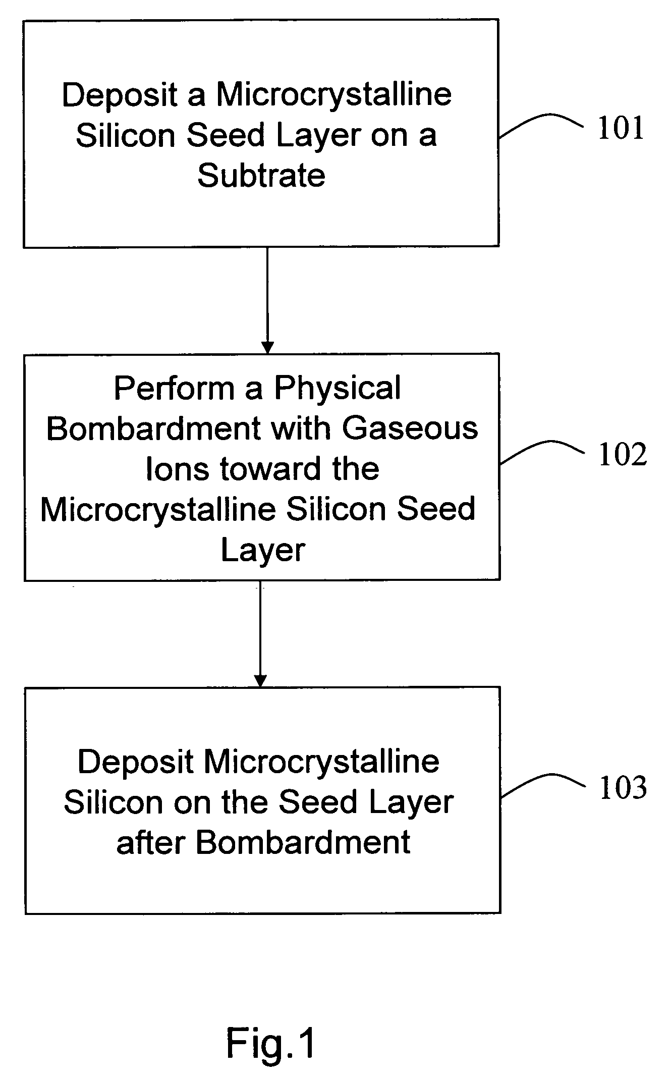
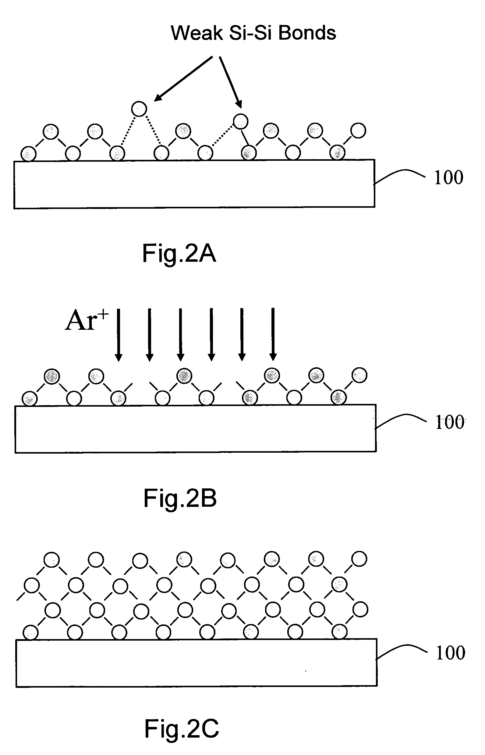
[0015]The present invention provides a method for forming a microcrystalline silicon thin film, employing a three-stage deposition process. At first, a microcrystalline silicon seed layer is deposited. Subsequently, ion bombardment is performed unto the microcrystalline silicon seed layer so that it obtains better crystallinity. Then, microcrystalline silicon is deposited on the microcrystalline silicon seed layer after bombardment, and a microcrystalline silicon thin film of a predetermined thickness is thus formed.

[0016]The method for forming a microcrystalline silicon thin film of the present invention will be described in details with following preferred embodiments and accompanying drawings.

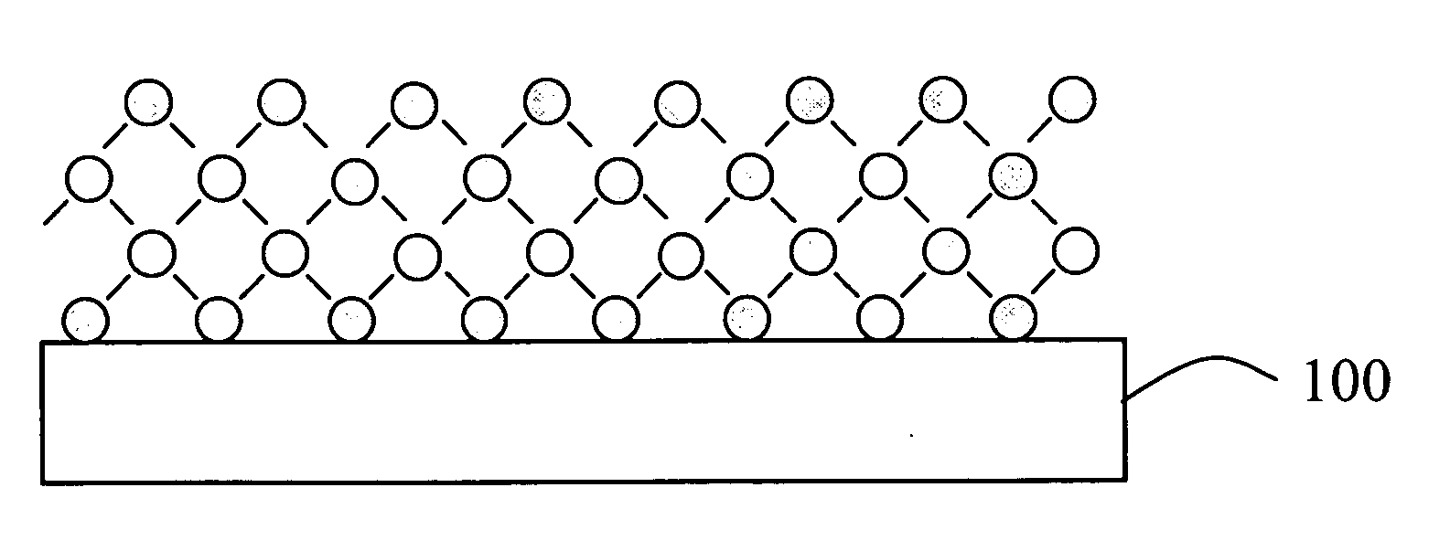
[0017]FIG. 1 is a process flow according to one preferred embodiment of the present invention. FIG. 2A through FIG. 2C is schematic views of growing the microcrystalline silicon thin film, which respectively correspond to various steps of the process flow of FIG. 1. Reference is now made to ...


PUM

PropertyMeasurementUnit
thicknessaaaaaaaaaa
thickaaaaaaaaaa
thicknessaaaaaaaaaa

Abstract

This invention provides a method for forming a microcrystalline silicon film, which employs a three-stage deposition process to form a microcrystalline film. A microcrystalline silicon seed layer is formed on a substrate. Gaseous ions are used to bombard a surface of the microcrystalline silicon seed layer. Microcrystalline silicon is formed on the microcrystalline silicon seed layer after the bombardment to a predetermined thickness.

Description

BACKGROUND OF THE INVENTION[0001]1. Field of the Invention[0002]This invention relates to a method for forming a microcrystalline silicon film, and more particularly to a method using a three-stage deposition process for forming a microcrystalline silicon film.[0003]2. Description of the Related Art[0004]Compared to a conventional amorphous silicon thin-film transistor (a-Si TFT), a low-temperature polycrystalline silicon thin-film transistor (LTPS-TFT) has a higher electron mobility and better reliability. Generally, a process of solid phase crystallization (SPC) or excimer laser annealing (ELA) is utilized for forming a polycrystalline silicon thin-film, wherein an amorphous silicon (a-Si:H) material is crystallized into a polycrystalline silicon (Poly-Si) by high-temperature annealing. However, the SPC process requires a higher crystallization temperature and thus needs silicon wafers or quartz glass as the substrates, which is expensive and unfavorable for large-area mass produc...

Claims


Application Information

Patent Timeline
Patent Type & Authority Applications(United States)
IPC IPC(8): H01L21/363
CPCC23C16/0272C23C16/24C23C16/56H01L21/02658H01L21/02532H01L21/02595H01L21/0262H01L21/0245
Inventor HUANG, JUNG-JIETSAI, CHENG-JUYEH, YUNG-HUI
Owner IND TECH RES INST
Why Eureka
Try Eureka