

Operational amplifier circuit, constant voltage circuit using the same, and apparatus using the constant voltage circuit
- Summary
- Abstract
- Description
- Claims
- Application Information
AI Technical Summary
Benefits of technology
Problems solved by technology
Method used
Image

Examples
Embodiment Construction
[0033]In the following, the present invention is described by way of embodiments and with reference to the drawings.
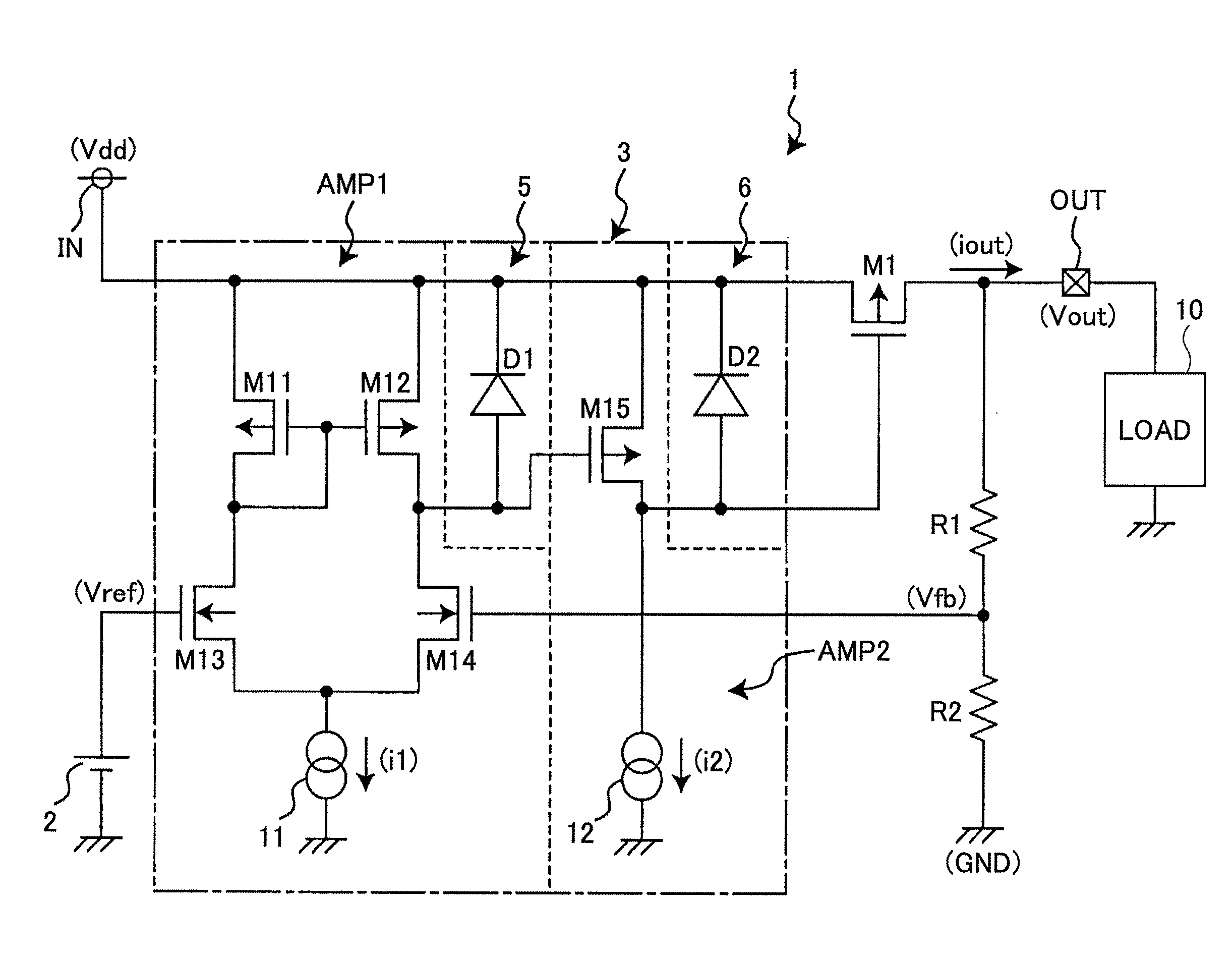
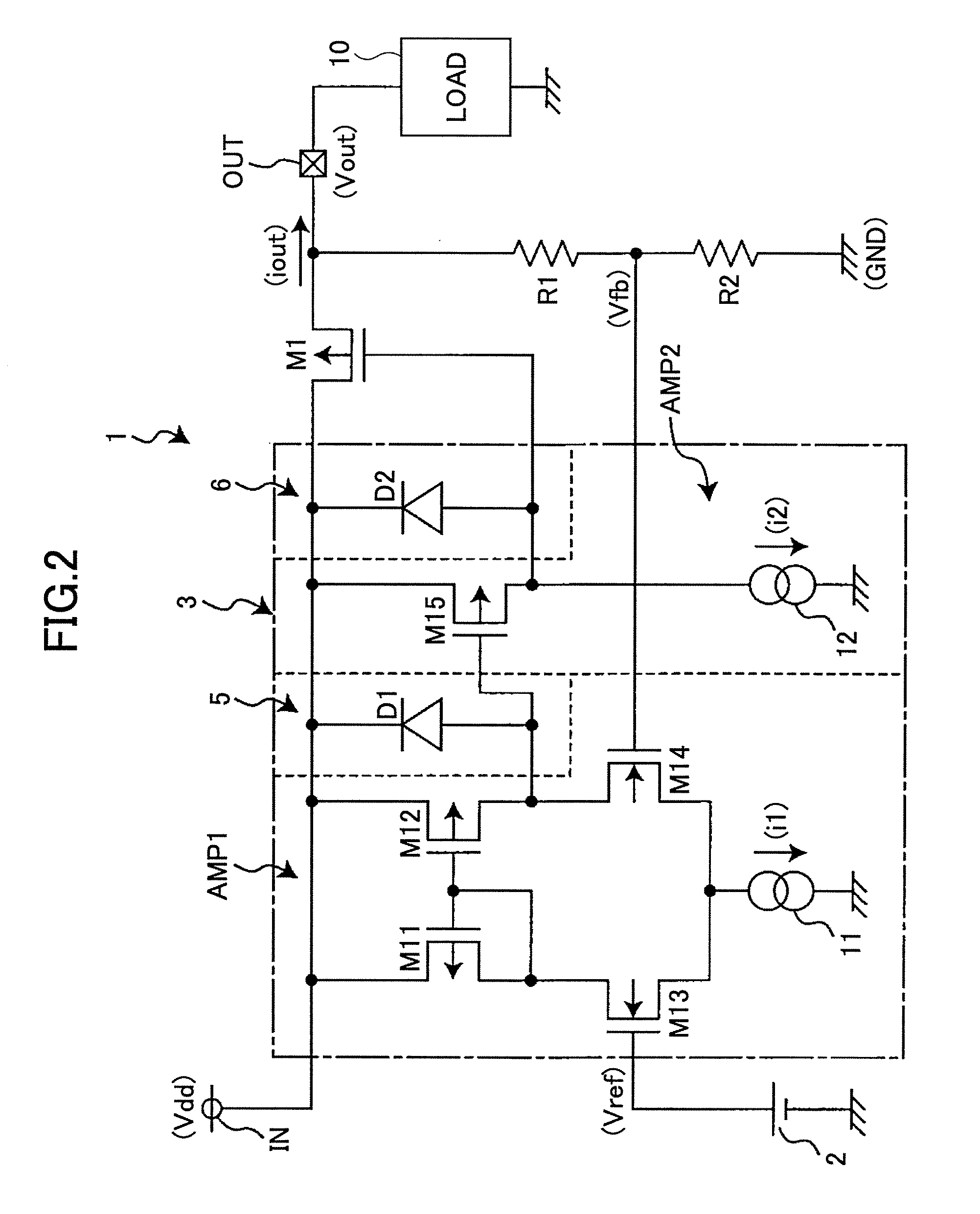
[0034]FIG. 2 shows a constant voltage circuit 1 according to an embodiment of the invention.
[0035]The constant voltage circuit 1 is configured to receive an input voltage Vdd at an input terminal IN and generate a predetermined constant voltage that is outputted as an output voltage Vout at an output terminal OUT. Between the output terminal OUT and a ground voltage GND, a load 10 is connected. The load 10 may be an apparatus having a predetermined function to which power is supplied from the constant voltage circuit 1. Examples of such an apparatus include an automotive electronic device, a copy machine, a printer, or other image forming apparatuses. In a preferred embodiment, such an apparatus may include the constant voltage circuit 1.
[0036]The constant voltage circuit 1 includes a reference voltage generating circuit 2 configured to generate a predetermined referen...
PUM
 Abstract
Description
Claims
Application Information