Fabrication method of an organic substrate having embedded active-chips

a technology of organic substrates and substrates, which is applied in the direction of printed circuits, semiconductor devices, semiconductor/solid-state device details, etc., can solve the problems of difficult to embed ic chips in substrates, difficult to implement light, slim, short and small structures, and difficult to implement i/os in chips, etc., to achieve enhanced package reliability and higher information capacity

Inactive Publication Date: 2009-02-12
KOREA ADVANCED INST OF SCI & TECH
View PDF3 Cites 44 Cited by
  • Summary
  • Abstract
  • Description
  • Claims
  • Application Information

AI Technical Summary

Benefits of technology

[0020]With the present invention, an integration technology for embedded active-chips based on a wafer level package process as well as a printed circuit board design, and fabricating technology for embedded active-chips and passivae components and a fabricating technology for a wafer level package in various forms to which conductive adhesives are applied, etc., can primarily be established. In the case of the printed circuit board for the embedded active-chips developed according to the present invention, it can be expected that the active-chips (semiconductor-chips) are embedded in the substrate so that the thickness of the package decreases and the interconnection length becomes short so that the reliability of the package is enhanced. Meanwhile, the present invention can be used in a system in package (SIP) of information and communication mobile product based on the printed circuit board including the embedded active-chips and passive components by using the printed circuit board fabricating technology for the embedded active-chips and passive components. This can significantly contribute to the provision of next generation core package components for higher speed Tbps-grade information and communication systems capable of processing higher capacity of information than possible in the prior art through the use of new IC-embdding technology.

Problems solved by technology

Among others, in the case of the wire bonding method (FIG. 3), it limits the number of I / Os in the chip and it is difficult to implement a light, slim, short, and small structure due to a wire shape and in the case of the electroplating method (FIG. 4), complex processes such as a seed layer deposition process, a thick film photo resist (PR) coating, and an exposure process, a plating process, an etching process, etc. are needed.
Even in the case of the flip chip interconnection method using the solder bumps (FIG. 5), it is difficult to embed the IC chips in the substrate due to complex processes, that is, there should be performed a solder flux coating process, an alignment process of chip and substrate, a solder reflow process, a flux cleaning process, an underfill coating process, and a curing process, etc.
In particular, it is very difficult to dispense underfill materials into the inside of the layer having the dented cavities and it should be subject to several processes which thus increase the cost.
However, until now it has been no attempt to fabricate an organic substrate with embedded active-chips using the conductive adhesives.
Therefore, since it is very difficult to perform the process of previously prelaminating the conductive adhesives to such an uneven structure and removing releasing film, it is not easy to achieve the interconnection using the conductive adhesives to the printed circuit board having the embedded active-chips.

Method used


Image

  • Fabrication method of an organic substrate having embedded active-chips
  • Fabrication method of an organic substrate having embedded active-chips
  • Fabrication method of an organic substrate having embedded active-chips

Examples


Embodiment Construction

[0029]Hereinafter, the fabrication method of an organic substrate having embedded active-chips of the present invention will be described in detail with reference to the accompanying drawings. The following drawings are provided, by way of example, to sufficiently transfer the idea of the present invention to those skilled in the art. Therefore, the present invention is not limited to the following drawings and can be embodied in other forms. In addition, the same reference numerals are used to refer to the same parts throughout the specification.

[0030]At this time, unless the terms and scientific terminologies used in the specification are defined, they have meanings understood by those skilled in the art. The following description of known functions and configurations will be omitted so as not to obscure the subject of the present invention with unnecessary detail.

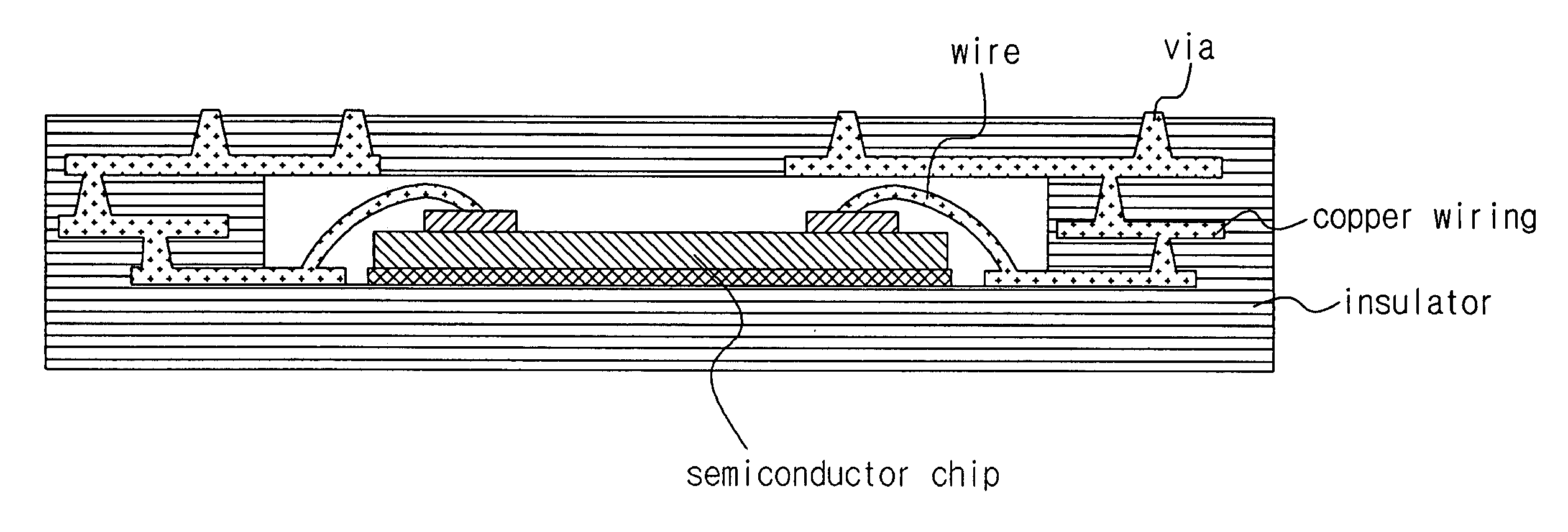
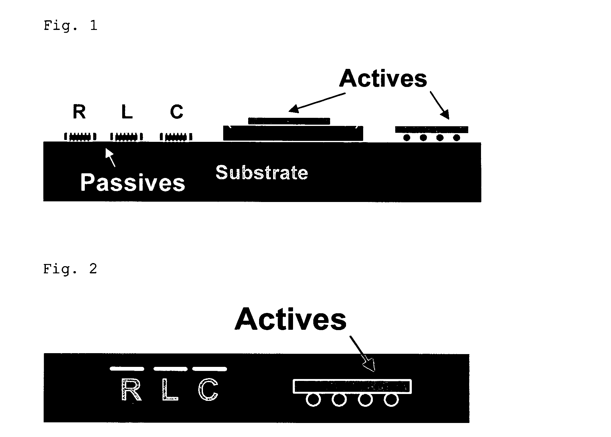
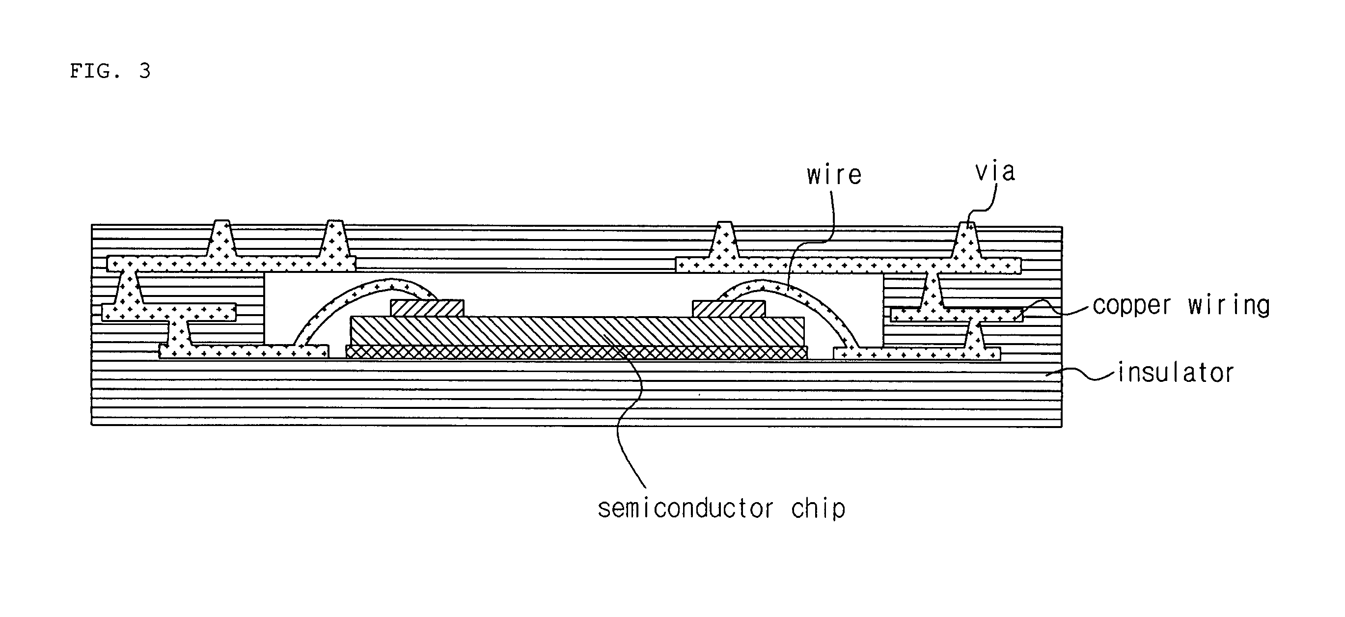
[0031]The present invention is a method that embed active-chips in a printed circuit board using a flip chip interconn...


PUM


Abstract

The fabrication method of an organic substrate having embedded active-chips such as semiconductor chips is disclosed. The present invention previously applies the conductive adhesives in a wafer state, makes them in a B-stage state, obtains individual semiconductor chips through dicing, and positions the individual semiconductor chips previously applied with the conductive adhesives in the cavities, making it possible to simultaneously obtain an electrical connection and a physical adhesion of the substrate and the semiconductor chips by means of a method of applying heat and pressure and stack the copper clad laminates on the upper portion of the substrate to which the semiconductor chips are connected. The present invention has advantages in processes such as a lead-free process, an environmental-friendly fluxless process, a low temperature process, ultra-fine pitch applications, etc., by mounting the active-chips through the flip chip interconnection using the non-solder bumps and the conductive adhesives.

Description

BACKGROUND OF THE INVENTION[0001]This application claims priority to Korean Patent Application No. 2007-0078457 filed on Aug. 6, 2007, in the Korean Intellectual Property Office, the entire contents of which are hereby incorporated by reference.[0002]1. Field of the Invention[0003]The present invention relates to a fabrication method of an organic substrate having embedded active-chips such as semiconductor chips.[0004]2. Description of the Related Art[0005]Electronic packaging technologies are a very important technology that determines the performance, size, price, and reliability of electronic products. The importance of the electronic packaging technologies has been highly recognized due to the recent trend of the high electrical performance and miniaturization of the electronic products. Among such electronic packaging technologies, a system in package (SIP) technology is to implement one system in a package. For this purpose, a silicon through-hole technology, a chip stacking ...

Claims


Application Information

Patent Timeline
Patent Type & Authority Applications(United States)
IPC IPC(8): H01L21/60
CPCH01L21/4857H01L2924/07811H01L23/5389H01L24/45H01L24/83H01L24/90H01L2224/1134H01L2224/13144H01L2224/16225H01L2224/32225H01L2224/45144H01L2224/48091H01L2224/48227H01L2224/73204H01L2224/73253H01L2224/73265H01L2224/83192H01L2224/838H01L2924/01002H01L2924/01004H01L2924/01005H01L2924/01013H01L2924/01014H01L2924/01029H01L2924/01059H01L2924/01078H01L2924/01079H01L2924/01082H01L2924/01322H01L2924/0781H01L2924/12044H01L2924/14H01L2924/15153H01L2924/1517H01L2924/15192H01L2924/16195H01L2924/19041H01L2924/19042H01L2924/19043H01L2924/30105H05K1/186H01L23/49822H01L24/29H01L24/32H01L24/48H01L2224/2919H01L2924/01006H01L2924/01033H01L2924/01076H01L2924/014H01L2924/0665H01L2924/01028H01L2924/00014H01L2924/00H01L2924/00012H01L24/73H01L23/12
Inventor PAIK, KYUNG-WOOKSON, HO-YOUNG
Owner KOREA ADVANCED INST OF SCI & TECH
Why Eureka
Try Eureka