Wafer holder, heater unit used for wafer prober having the wafer holder, and wafer prober having the heater unit

a heater unit and heater technology, applied in the field of heater units used for wafer probers and heater units, can solve the problems of long time to increase and decrease the temperature of the heater, the contact failure of the wafer and the probe pin, and the drawback of improving the throughput, so as to achieve better thermal uniformity of the wafer

Inactive Publication Date: 2009-02-26
SUMITOMO ELECTRIC IND LTD
View PDF2 Cites 368 Cited by
  • Summary
  • Abstract
  • Description
  • Claims
  • Application Information

AI Technical Summary

Benefits of technology

[0015]In view of the situations of the conventional art as described above, an object of the present invention is to provide a wafer holder suitably used in a wafer prober for inspecting electric characteristics of a wafer, which prevents positi...

Problems solved by technology

At the time of measurement, however, a prober referred to as a probe card having a number of electrode pins for electric conduction is pressed to the wafer with a force of several tens to several hundreds kgf, and therefore, when the heater is thin, the heater would possibly be deformed, resulting in contact failure between the wafer and the probe pin.
Therefore, it has been necessary to use a thick metal plate having the thickness of at least 15 mm for the heater, in order to maintain rigidity of the heater, and therefore, it takes long time to increase and decrease the temperature of the heater, which is a significant drawback in improving the throughput.
As recent chips come to have higher outputs, it is possible that a chip generates considerable heat during measurement of electric characteristics, and in some situations, the chip might be broken by self-heating.
There is a problem, however, that when the wafer is heated to a prescribed temperature, that is, to about 100 to 200° C., the heat is transferred to the driving system, and metal components forming the driving system thermally expand, degrading positional accuracy.
Further, along with the increase in load at the time of probing, rigidity of the prober itself mounting the wafer has come to be required.
Specifically, when the wafer prober itself deforms because of the load at the time of probing, uniform contact of the pins of probe card with the wafer would fail and inspection b...

Method used


Image

  • Wafer holder, heater unit used for wafer prober having the wafer holder, and wafer prober having the heater unit
  • Wafer holder, heater unit used for wafer prober having the wafer holder, and wafer prober having the heater unit
  • Wafer holder, heater unit used for wafer prober having the wafer holder, and wafer prober having the heater unit

Examples


examples

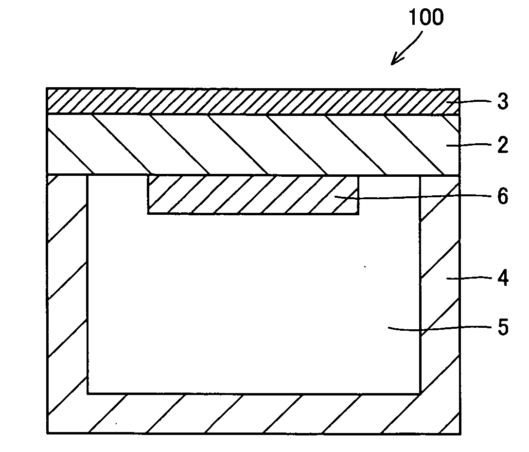
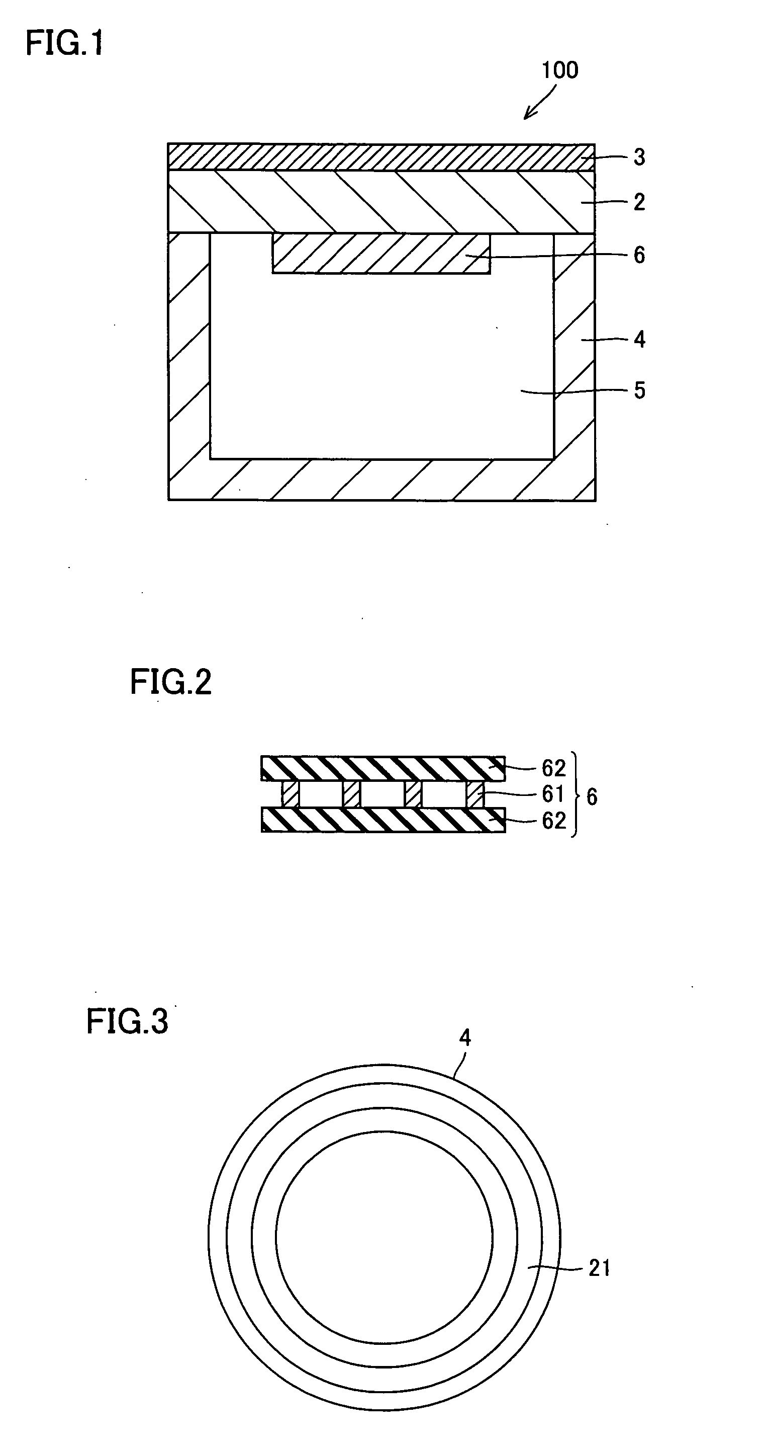
[0118]Six Si—SiC substrates having the diameter of 310 mm and the thickness of 15 mm and different water absorption were prepared as the material for chuck top 2. On the wafer-mounting surface of these Si—SiC substrates, suction trenches in the shape of concentric circles, suction holes and a suction inlet for vacuum chucking a wafer were formed, and the wafer-mounting surface was nickel-plated to form chuck top conductive layer 3. Thereafter, chuck top conductive layer 3 was polished and finished to have the overall warp amount of 10 μm and surface roughness Ra of 0.02 μm, and thus, chuck tops 2 were formed.

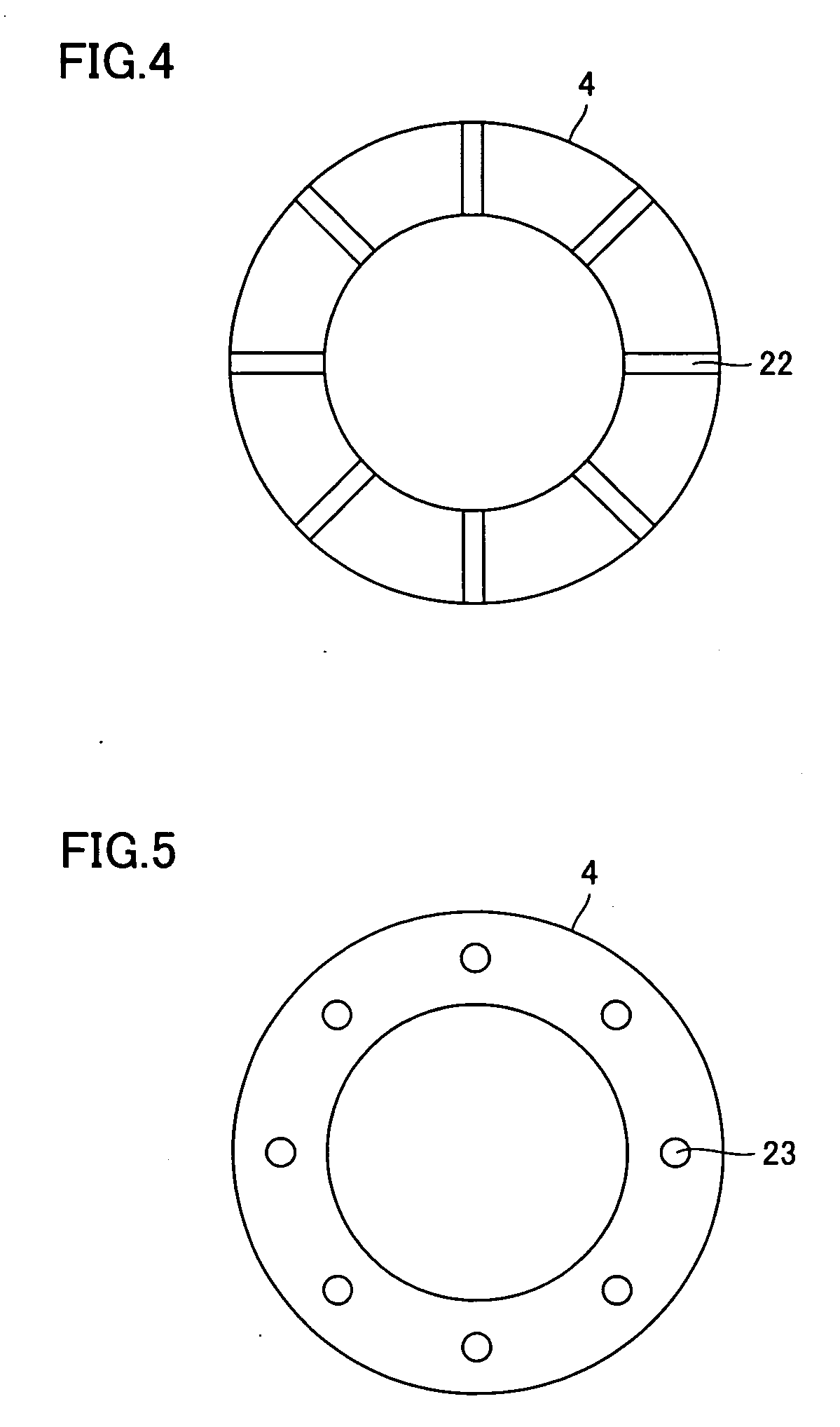
[0119]On the other hand, six mullite-alumina composite bodies of a pillar shape having the diameter of 310 mm and thickness of 40 mm were prepared as the material for supporter 4. One flat surface of these mullite-alumina composite bodies was counter-bored to have the inner diameter of 295 mm and the depth of 20 mm, and thus, supporters 4 of hollow cylindrical shape with a botto...


PUM


Abstract

A wafer holder that prevents positional deviation of the wafer mounted on the wafer-mounting surface of a chuck top and enables better thermal uniformity of the wafer, as well as a heater unit including the wafer holder and a wafer prober mounting these are provided. The wafer holder has a chuck top mounting and fixing the wafer and a supporter supporting the chuck top, and the chuck top has water absorption of at least 0.01% and preferably at least 0.1%. Preferable material of the chuck top is a composite of metal and ceramics, and particularly, a composite of aluminum and silicon carbide, or a composite of silicon and silicon carbide.

Description

BACKGROUND OF THE INVENTION[0001]1. Field of the Invention[0002]The present invention relates to a wafer holder suitably used in a wafer prober for inspecting electric characteristics of a wafer, a heater unit for a wafer prober including the wafer holder, and to a wafer prober including the heater unit.[0003]2. Description of the Background Art[0004]Conventionally, in a process for inspecting a semiconductor wafer, a semiconductor wafer (wafer) as an object of processing has been subjected to heat treatment (burn-in). Specifically, by heating the wafer to a temperature higher than the normal temperature of use, degradation of a possibly defective semiconductor chip is accelerated and the defective chip is removed, in order to prevent defects after shipment. In the burn-in process, after semiconductor circuits are formed on the semiconductor wafer and before the wafer is cut into individual chips, electrical characteristics of each semiconductor chip are measured while the semicondu...

Claims


Application Information

Patent Timeline
IPC IPC(8): H05B3/68
CPCH05B3/148H01L21/67103
Inventor AWAZU, TOMOYUKIITAKURA, KATSUHIRONATSUHARA, MASUHIRONAKATA, HIROHIKO
Owner SUMITOMO ELECTRIC IND LTD
Why Eureka
Try Eureka