
ZnSe scintillators

a zinc selenide and scintillator technology, applied in the field of microcolumnar zinc selenide scintillators, can solve the problems of difficult prediction or production of specific compositions/formulations and structures having both scintillation and the capability of imaging at a high resolution

Active Publication Date: 2009-02-26
RADIATION MONITORING DEVICES
View PDF8 Cites 11 Cited by
  • Summary
  • Abstract
  • Description
  • Claims
  • Application Information

AI Technical Summary

Benefits of technology

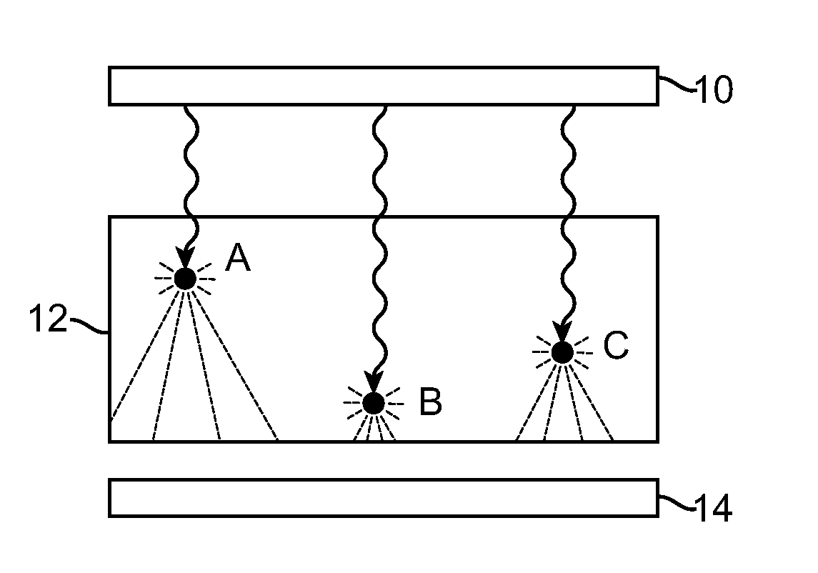
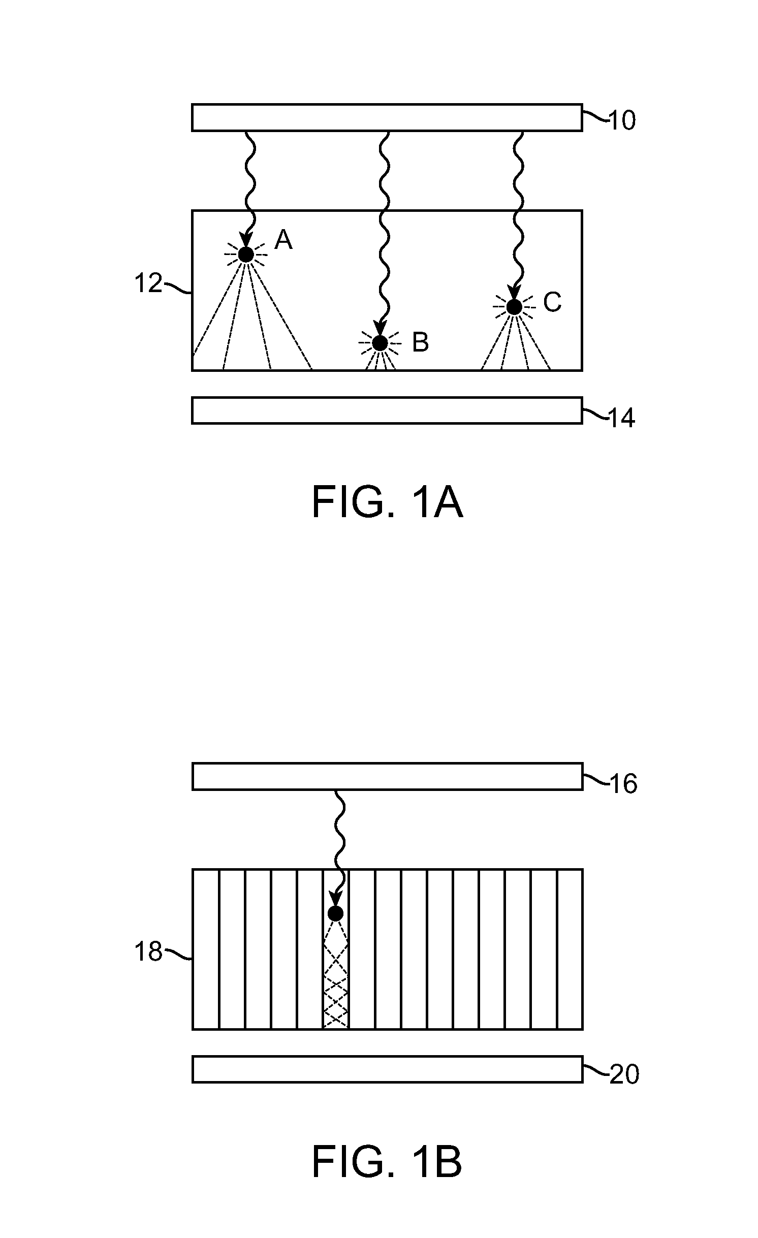
[0010]Thus, in one embodiment, the present invention includes a scintillator including a microcolumnar scintillator material including zinc selenide (ZnSe) and a dopant. Various dopants can be included in the microcolumnar scintillator of the present invention including, for example, tellurium (Te), oxygen (O), and copper (Cu). The improved light channeling and resolution characteristics of the disclosed microcolumnar scintillators allow for use of thicker scintillators, providing additional advantages of increased absorption efficiency with thicker scintillator with minimized loss of resolution. Thus, the microcolumnar scintillators of the present invention provide high spatial resolution scintillators as well as efficient scintillators, or scintillators having a high absorption efficiency. Additionally, the disclosed microcolumnar scintillators will typically have a high light output and preserve the other desirable properties of ZnSe as enumerated below.
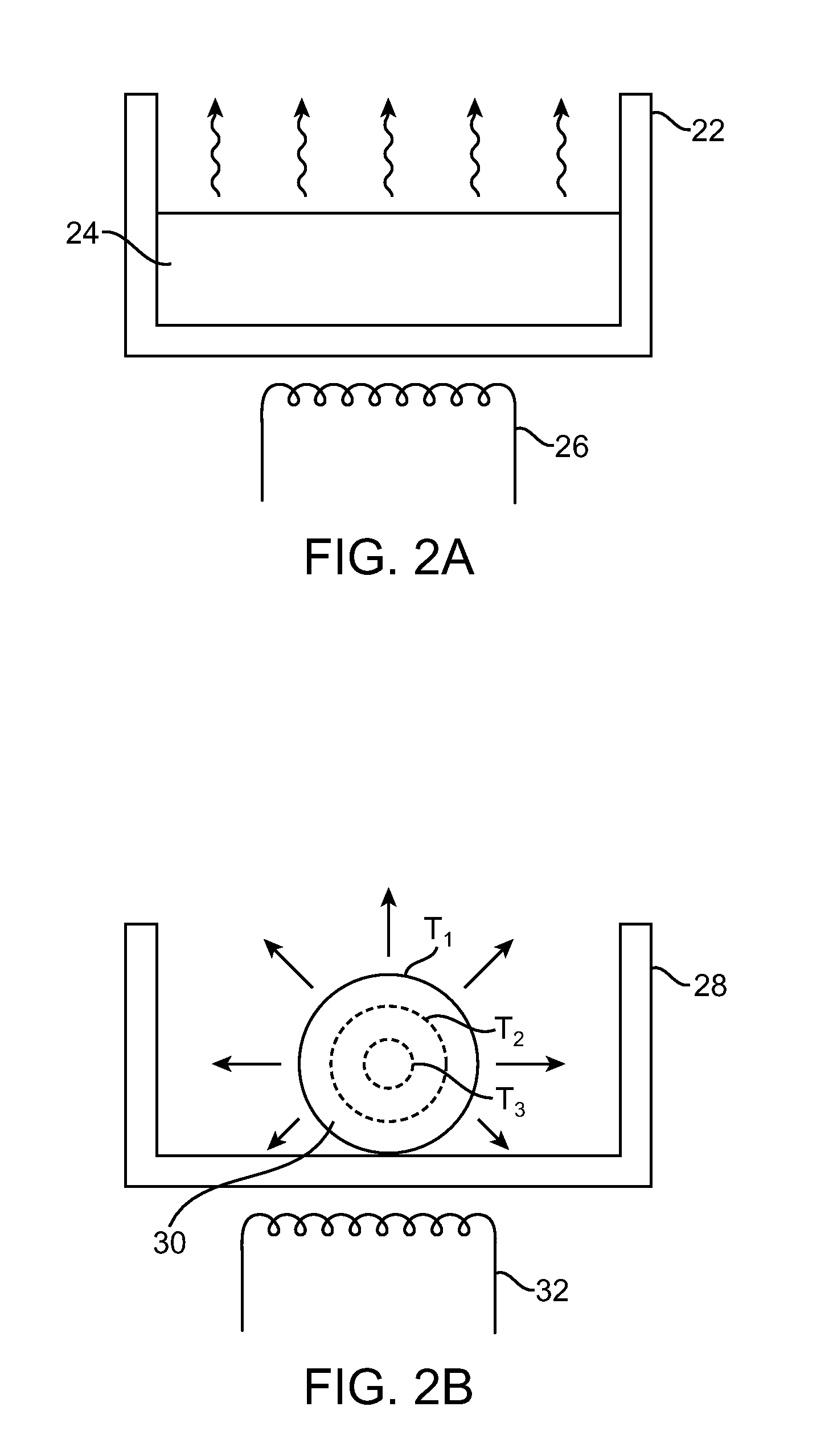
[0015]Advantages of the microcolumnar scintillators of the invention and the sublimation deposition growth (e.g., PVD) technique for fabricating the ZnSe scintillator as described herein include the following: The material can be grown in a microcolumnar form needed for numerous high spatial resolution imaging applications. The fabrication techniques of the present invention allow preservation of the stoichiometry of the deposited film, even though the source material can include compounds having relatively large differences in vapor pressures and sticking coefficients. The sublimation deposition technique allows fabrication of large area (e.g., 50×50 cm2 or larger) screens of the required thickness in a cost effective manner. Films may be fabricated on a variety of substrates, including rigid or flexible, opaque or transparent substrates of any shape, thereby making them adaptable for incorporation in a variety of detector configurations.

Problems solved by technology

These requirements are often not met by many of the commercially available scintillators.
While general classes of chemical compositions may be identified as potentially having some attractive scintillation characteristic(s), specific compositions / formulations and structures having both scintillation characteristics and physical properties necessary for actual use in scintillation spectrometers and various practical applications, as well as capability of imaging at a high resolution, have proven difficult to predict or produce.
Specific scintillation properties are not necessarily predictable from chemical composition alone, and preparing effective scintillators from even candidate materials often proves difficult.
With the advent of X-ray CT in the 1970's, a major commercial field emerged as did a need for different scintillators, as NaI(Tl) was not able to meet the requirements of CT imaging.
As the methodology of scintillator development evolved, new materials have been added, and yet, specific applications, particularly those requiring high resolution imaging, are still hampered by the lack of scintillators suitable for particular applications.
While it is may be possible to reject a potential scintillator for a specific application based solely on composition, it is not possible to predict whether a material with promising composition will produce a scintillator with the desired properties.
The latter method is complex, as it requires a specialized carbon fiber-lined growth furnace, high temperature heaters to reach ˜1600 C (needed for congruent melting of the material), and a well-balanced temperature gradient to foster nucleation and defect-free crystal growth.
The tremendous complexity of the current methods results in yield problems and a high cost for the scintillator.
However, very little or no work has been reported on the synthesis of efficient luminescent ZnSe (i.e., with dopants like Te) for X-ray / γ-ray detection.
Additionally, this technique is limited to producing thin films, for example, measuring 1 μm or less in thickness, which can be inadequate for detecting X-rays due to inefficient absorption.
Furthermore, this type of process is expensive and does not permit formation of a scintillator structure capable of both high detection efficiency and high-resolution imaging.
Besides crystalline form, ZnSe:Te can be synthesized in powder form, but powdered screens are limited in use due to a substantial tradeoff between detection efficiency, which increases with increasing scintillator thickness, and spatial resolution, which decreases with increasing scintillator thickness, inherent in the light diffusion process.
Unfortunately, the much thicker powdered screens not only result in light loss due to internal scattering, but also result in poor spatial resolution.
ZnSe material used in IR windows is manufactured by chemical vapor deposition (CVD), however, it does not include any activator doping and consequently is a non-scintillator.

Method used


Image

  • ZnSe scintillators
  • ZnSe scintillators
  • ZnSe scintillators

Examples


examples

[0061]The present examples provides characterization of microcolumnar, doped ZnSe scintillators according to an embodiment of the present invention. The examples provided herein are offered by way of illustration, not by way of limitation.

[0062]In one embodiment, films of ZnSe:Te in the range of 25 μm to 85 μm thickness were produced and tested for performance characteristics, the results of which are further described herein below. For detection of low energy X-rays, these films offered >80% X-ray absorption; up to a factor of three greater light emission (90,000 to 180,000 ph / MeV) compared to the highest known conversion efficiency scintillators; fast decay time in the microsecond range; virtually no afterglow, and an excellent radiation resistance. Furthermore, the 550 nm to 900 nm light emission, peaking at about 650 nm to 750 nm depending on the dopant concentration, of ZnSe:Te provides an excellent match to the quantum efficiency of the EMCCD sensor that are preferred as photo...


PUM

PropertyMeasurementUnit
thicknessaaaaaaaaaa
diameteraaaaaaaaaa
pressureaaaaaaaaaa

Abstract

The present invention relates to a microcolumnar zinc selenide (ZnSe) scintillator and uses thereof, and methods of fabrication of microcolumnar scintillators using sublimation-based deposition techniques. In one embodiment, the present invention includes a scintillator including a microcolumnar scintillator material including zinc selenide (ZnSe) and a dopant. The microcolumnar scintillators of the present invention provide improved light channeling and resolution characteristics, thereby providing high spatial resolution, highly efficient scintillators.

Description

BACKGROUND OF THE INVENTION[0001]The present invention relates to a scintillator. More specifically, the present invention relates to a microcolumnar zinc selenide scintillator and use thereof, and methods of fabrication of microcolumnar scintillators using sublimation-based deposition techniques.[0002]Scintillation spectrometers are widely used in detection and spectroscopy of energetic photons (e.g., X-rays and y-rays). Such detectors are commonly used, for example, in nuclear and particle physics research, medical imaging, diffraction, non destructive testing, nuclear treaty verification and safeguards, nuclear non-proliferation monitoring, and geological exploration.[0003]Important requirements for the scintillation materials used in these applications include high light output, transparency to the light it produces, high stopping efficiency, fast response, good proportionality, low cost and availability in large volume. These requirements are often not met by many of the commer...

Claims


Application Information

Patent Timeline
Patent Type & Authority Applications(United States)
IPC IPC(8): G01T1/20
CPCG01T1/202
Inventor NAGARKAR, VIVEKGAYSINSKIY, VALERIY
Owner RADIATION MONITORING DEVICES
Learn More