Mis gate structure type HEMT device and method of fabricating mis gate structure type HEMT device

a gate structure and gate structure technology, applied in the direction of semiconductor devices, basic electric elements, electrical apparatus, etc., can solve the problems of inability to achieve low on-resistance, inability to obtain low on-resistance, inability to ensure high two-dimensional electron gas concentration, etc., to achieve low access resistance and low on-resistance

Inactive Publication Date: 2009-02-26
NGK INSULATORS LTD
View PDF2 Cites 43 Cited by
  • Summary
  • Abstract
  • Description
  • Claims
  • Application Information

AI Technical Summary

Benefits of technology

[0012]According to the present invention, sufficiently lowered access resistance in an access portion, that is, between a drain and a gate and between a gate and a source, is implemented by forming the two-dimensional electron gas region in the periphery of the hetero-jun...

Problems solved by technology

Further, in the case where HEMT devices are formed by techniques disclosed in the above-mentioned article 3 and article 4, the piezo-effect is suppressed due to thinning of an AlGaN barrier layer and therefore, there occurs a problem that sufficiently high two-dimensional electron gas concentration cannot be assured and a low on-resist...

Method used


Image

  • Mis gate structure type HEMT device and method of fabricating mis gate structure type HEMT device
  • Mis gate structure type HEMT device and method of fabricating mis gate structure type HEMT device
  • Mis gate structure type HEMT device and method of fabricating mis gate structure type HEMT device

Examples


first embodiment

Configuration of HEMT Device

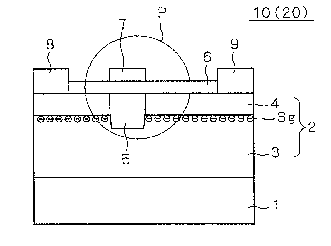
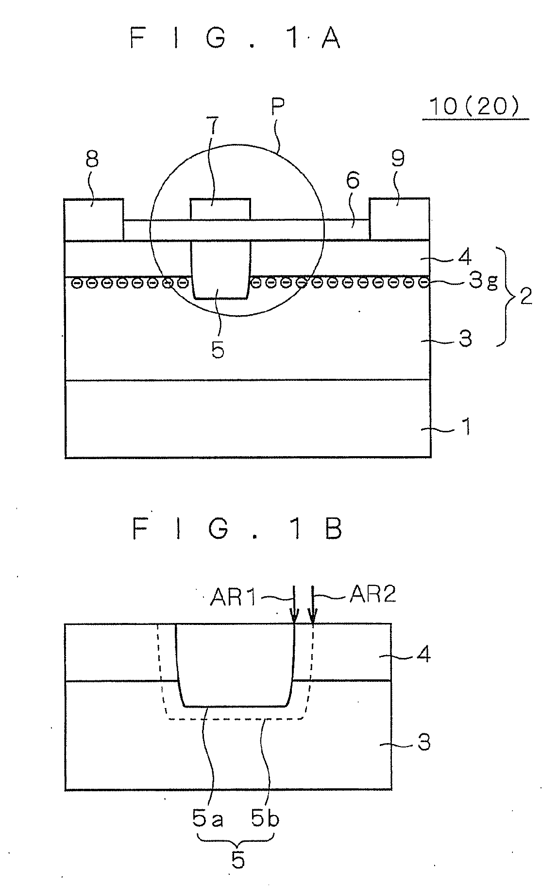
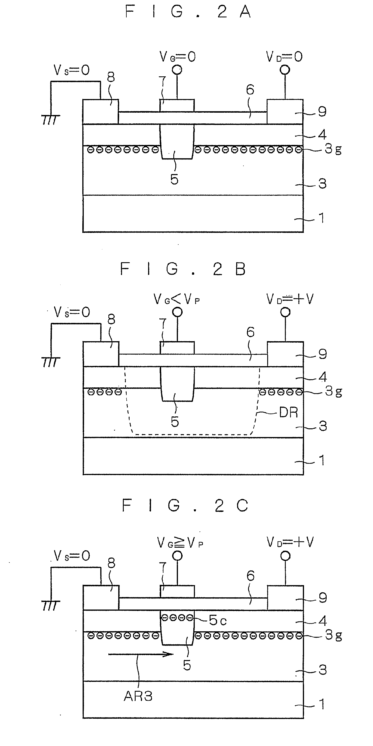
[0030]FIGS. 1A and 1B are views schematically showing a configuration of a HEMT device 10 according to a first embodiment. FIG. 1A is a typical cross-sectional view of an entire configuration of the HEMT device 10. As shown in FIG. 1A, from a schematic viewpoint, the HEMT device 10 according to the embodiment is provided with a semiconductor layer 2, an insulating layer 6, a gate electrode 7, a source electrode 8, and a drain electrode 9 on a substrate 1. That is, the HEMT device 10 has a MIS gate structure configured by forming the insulating layer 6 between the semiconductor layer 2 and the gate electrode 7. Further, the semiconductor layer 2 is provided with a base layer 3, a barrier layer 4, and a P-type region 5.

[0031]Use of a single crystal 6H—SiC substrate is one of preferable examples for the substrate 1, however, materials are not particularly limited as long as they can be used to form Group III nitride semiconductor layers such as the base laye...

second embodiment

[0072]In the first embodiment described above, an aspect in which the base layer 3 is formed as a high resistance layer having conductivity of N-type and a high specific resistance of 1×10⁷ Ωcm or more are shown. However, the base layer 3 may be composed of Group III nitride having conductivity of P-type instead of this aspect. For example, the base layer 3 may be composed of GaN containing Mg as an acceptor. In this case, the layer is preferably formed in a manner that a hole concentration at room temperature is adjusted to be 1×10¹⁶ / cm3 to 1×10¹⁸ / cm3, for example, about 2×10¹⁶ / cm3.

[0073]Since such a HEMT device 20 has almost same configuration as that of the HEMT device 10 according to the first embodiment shown in FIG. 1A, the detailed description of the respective parts are omitted. However, the configuration of the P-type region 5 is slightly made different.

[0074]FIG. 4 is a view typically showing a configuration of a P-type region in the HEMT device 20. In the HEMT device 20, ...

third embodiment

[0079]FIG. 5 is a view schematically showing a configuration of a HEMT device 30 according to a third embodiment. In the present embodiment, the same symbols are assigned to the constituent components having the same functional effects as those of the constituent elements of the HEMT device 10 according to the first embodiment and detailed descriptions about the constituent components are omitted. Although the HEMT device 30 is same as the HEMT device 10 according to the first embodiment in a point that both have the MIS gate structure having the insulating layer 6 between the semiconductor layer 2 and the gate electrode 7, the HEMT device 30 differs in a point that an AlN layer (AlN spacer layer) 31 made of AlN is inserted between the base layer 3 and the barrier layer 4.

[0080]The AlN layer 31 is inserted for suppressing a decrease in an electron mobility due to partial immersion of the two-dimensional electron gas region 3g in the barrier layer 4. Accordingly, a further high mobil...


PUM


Abstract

A normally-off operation type HEMT device excellent in characteristics can be realized. A two-dimensional electron gas region is formed in a periphery of a hetero-junction interface of a base layer and a barrier layer, so that access resistance in an access portion, that is, between a drain and a gate and between a gate and a source is sufficiently lowered, and at the same time, a P-type region is formed immediately under the gate. This realizes a normally-off type HEMT device having a low on-resistance. Further, when a film thickness of an insulating layer is defined as t (nm) and a relative permittivity of a substance forming the insulating layer is defined as k, a threshold voltage as high as +3 V or more can be attained by satisfying k/t≦0.85 (nm−1).

Description

BACKGROUND OF THE INVENTION[0001]1. Field of the Invention[0002]The present invention relates to a MIS gate structure type HEMT device and particularly a normally-off type HEMT device.[0003]2. Description of the Background Art[0004]Since a nitride semiconductor has a high insulation breakdown electric field and a high saturated electron velocity, the nitride semiconductor has attracted attention as a semiconductor material for high frequency / high power devices of next generation. In particular, a layered structure of Group III nitride materials such as AlGaN / GaN and AlInN / GaN can store a high concentration of two-dimensional electron gas in a layered interface due to significant polarization effects (spontaneous polarization effect and piezo-polarization effect) peculiar to the nitride materials. Development of a high electron mobility transistor (HEMT) using this characteristic has been actively carried out. (see “Highly Reliable 250W GaN High Electron Mobility Transistor Power Amp...

Claims


Application Information

Patent Timeline
IPC IPC(8): H01L29/778H01L21/336
CPCH01L29/1033H01L29/1066H01L29/2003H01L29/7787H01L29/517H01L29/66462H01L29/4232
Inventor MIYOSHI, MAKOTOTANAKA, MITSUHIRO
Owner NGK INSULATORS LTD
Why Eureka
Try Eureka