
Complementary logic circuit

a logic circuit and circuit technology, applied in logic circuits characterized by logic functions, logic circuits using specific components, pulse techniques, etc., can solve problems such as increasing power consumption, increasing power consumption, and affecting the performance of circuits with planar gate electrodes using cmos technology. performance superior

Active Publication Date: 2009-02-26
IBM CORP
View PDF4 Cites 7 Cited by
  • Summary
  • Abstract
  • Description
  • Claims
  • Application Information

AI Technical Summary

Benefits of technology

[0049]According to the present invention, it is possible to achieve performance superior to the current CMOS technology in fine design and power consumption and obtain a logic circuit of a system consistent with the implementation of a classical computer using existing sequential circuits. Further, the present invention can provide a technique which obtains the logic circuit without using a majority logic and causes no trade-off between input / output isolation and a gain, that is, obtains input / output separation and an input gain.

Problems solved by technology

However, the FETs with the planar gate electrode using CMOS technology are expected to reach a technical limit in about 2016.
That is, various undesirable effects caused by a shorter gate length (and thinner oxide thickness) become more pronounced as MOSFETs advance in fine design rule.
A large off current increases power consumption.
Considering that an operating frequency (clock frequency) tends to increase, an increase in power consumption per area is a serious problem.
The second approach is to study principles and cannot make considerable progress overnight.
It is necessary to make steady efforts and satisfactory results are not obtained at present.

Method used


Image

  • Complementary logic circuit
  • Complementary logic circuit
  • Complementary logic circuit

Examples


Embodiment Construction

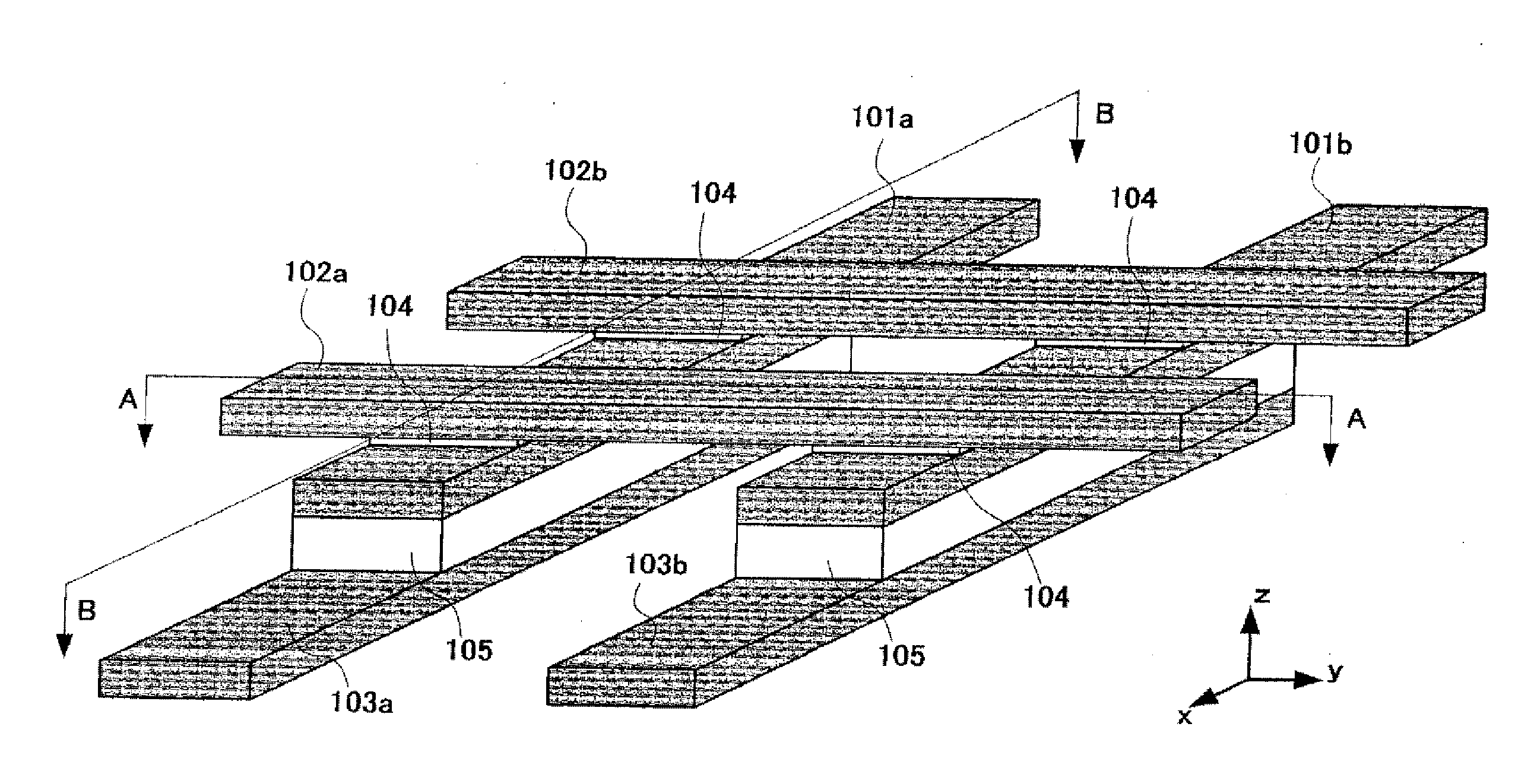
[0050]An embodiment of the present invention will be specifically described below in accordance with the accompanying drawings. FIG. 5 is a perspective view showing an example of a quantum logic device according to an embodiment of the present invention. FIG. 6 is a sectional view taken along line A-A of FIG. 5. FIG. 7 is a sectional view taken along line B-B of FIG. 5.

[0051]The quantum logic device of the present embodiment includes a first conducting member 101a, a first conducting member 101b, a second conducting member 102a, a second conducting member 102b, a third conducting member 103a, and a third conducting member 103b. The quantum logic device shown in FIG. 5 has two quantum logic devices and will be described in detail later. An insulating member 104 is formed between the first conducting members 101a and 101b and the second conducting members 102a and 102b, and an insulating member 105 is formed between the first conducting members 101a and 101b and the third conducting m...


PUM


Abstract

A quantum device comprises first conductive members and second conductive members confining carriers in the z direction and having two dimensional electron gas on the xy plane. Third conductive members generating an electric field having an effect on the first conductive members. An insulating member easily passing a tunnel current between the first conductive members and the second conductive members. Another insulating member hardly passing a tunnel current between the first conductive members and the third conductive members. An electric field generated by a potential applied to the third conductive members has an effect on the sub-band of the first conductive members.

Description

FIELD OF THE INVENTION[0001]The present invention relates to a quantum device, a quantum logic device, a method of driving the quantum logic device, and a logic circuit. Particularly the present invention relates to a technique effectively used for a quantum device which operates stably with low power consumption even in a fine scaled dimension theoretically unavailable in silicon MOSFETs having become mainstream at present, and which can constitute a complementary logic circuit of a system consistent with the implementation of a classical computer using existing sequential circuits.BACKGROUND ART[0002]It is already known that CMOSFETs (CMOS Field Effect Transistors) using CMOS (Complementary-Metal Oxide Semiconductor) technology are mainly used as the logic elements of current information processing systems such as computers. Further, it is known that finer design rules have been advanced for CMOSFETs with great effort in response to the need for higher performance of information p...

Claims


Application Information

Patent Timeline
Patent Type & Authority Applications(United States)
IPC IPC(8): H03K19/20H01L29/06H01L29/66H01L29/772H01L29/88H03K19/02
CPCH01L29/772Y10S977/774Y10S977/762H01L29/88H01L29/06H01L29/66
Inventor KATAYAMA, YASUNAO
Owner IBM CORP
Learn More