
Organic semiconducting material, and film, organic electronic device and infrared dye composition each including said material

a semiconducting material and organic technology, applied in the direction of organic semiconductor devices, porphines/azaporphines, final product manufacturing, etc., can solve the problems of low energy conversion efficiency of organic thin-film solar cells, many materials known as infrared dyes suffer decomposition, and cannot match silicon-utilized solar cells in photoelectric conversion capability, etc., to achieve high stability

Active Publication Date: 2009-02-26
FUJIFILM CORP
View PDF5 Cites 8 Cited by
  • Summary
  • Abstract
  • Description
  • Claims
  • Application Information

AI Technical Summary

Benefits of technology

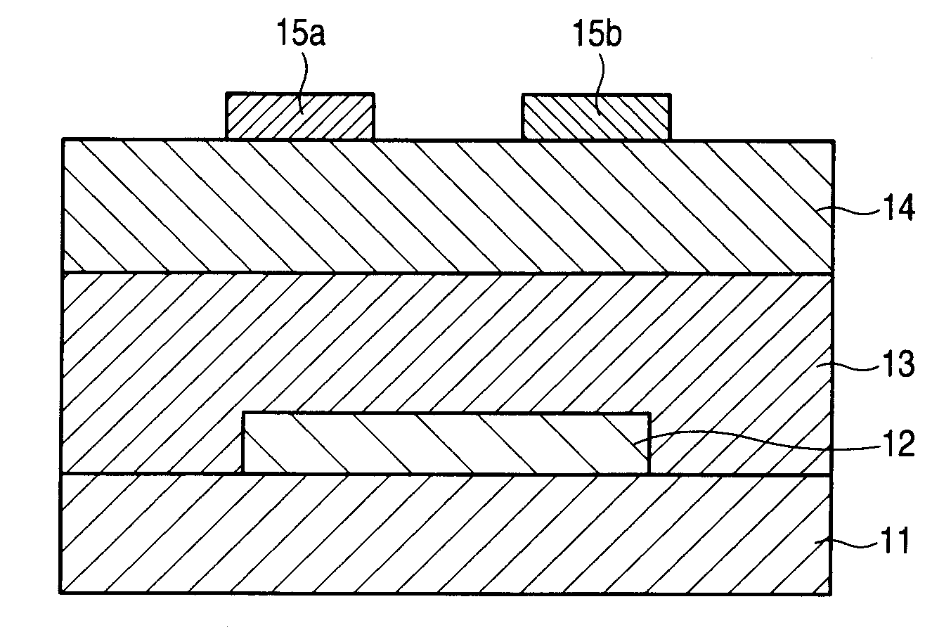
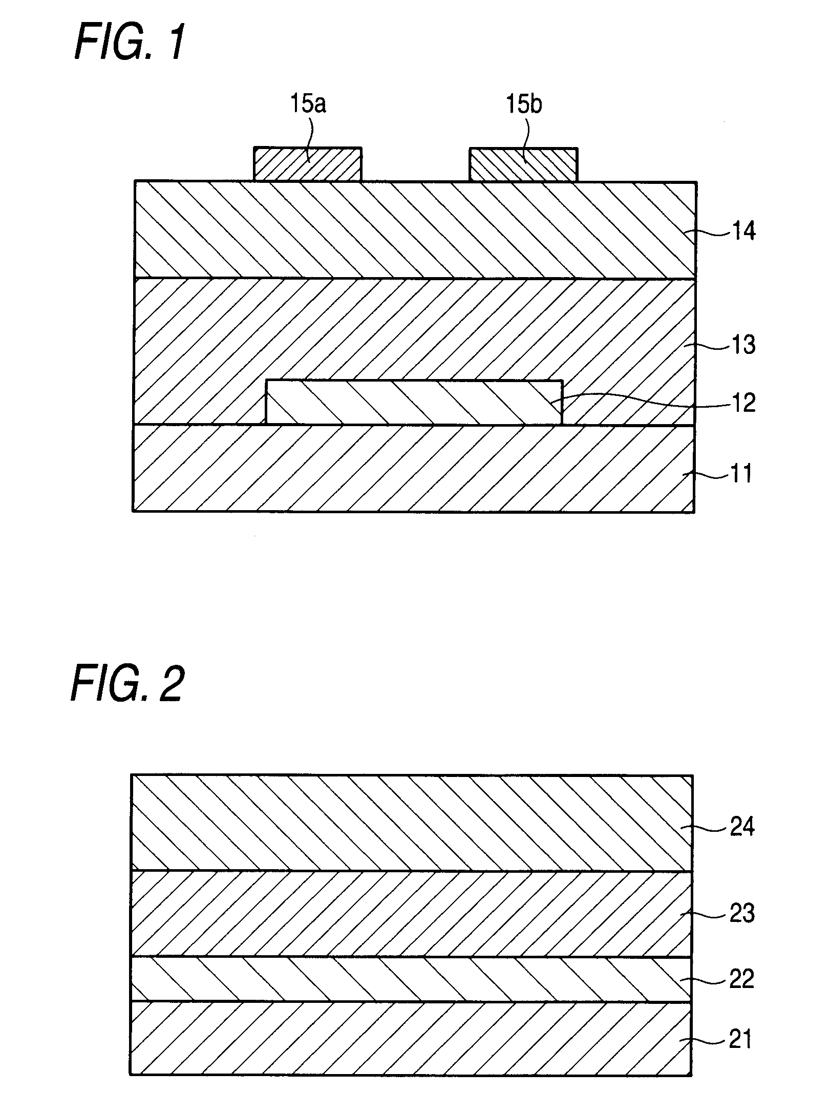
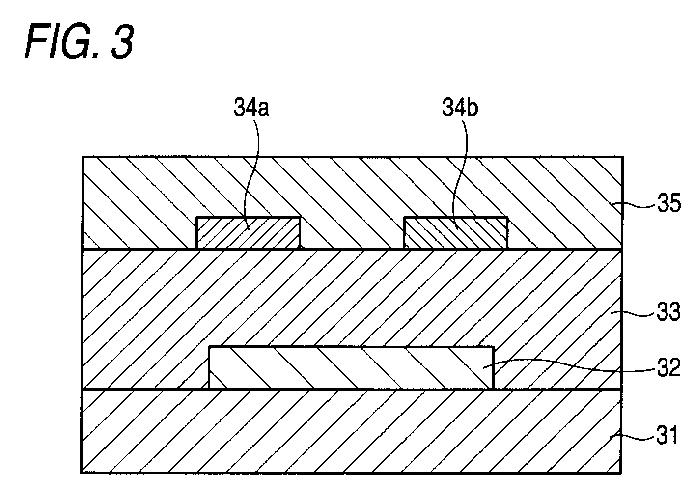
[0008]The invention is made in view of the technical background mentioned above, and aims to provide a high-performance organic semiconducting material that can be formed into film by both a vacuum process and a solution process, has high stability and shows light absorption and photoelectric conversion characteristics in the infrared region, and further to provide a variety of high-performance organic electronic devices (especially a photoelectric transducer and an organic transistor) each using such an organic semiconducting material.

Problems solved by technology

However, this case can not match silicon-utilized solar cells in photoelectric conversion capability, so further improvement in performance is required thereof.
A cause of low energy conversion efficiency of organic thin-film solar cells consists in that the organic materials used therein show light absorption and photoelectric conversion in wavelength regions narrower than the wavelength region of the light radiating from the sun, and that they fail to utilize light in long wavelength region (infrared region) in particular (Kaku Uehara & Susumu Yoshikawa (editors), Yuki Hakumaku Taiyo Denchi no Saishin Gijutu (Leading-edge Technology for Thin Film Organic Photovoltaic Cells), pp.
Many of materials known as infrared dyes suffer decomposition by heating, and only limited number of infrared dyes can be formed into film by a vacuum process.

Method used


Image

  • Organic semiconducting material, and film, organic electronic device and infrared dye composition each including said material
  • Organic semiconducting material, and film, organic electronic device and infrared dye composition each including said material
  • Organic semiconducting material, and film, organic electronic device and infrared dye composition each including said material

Examples


examples

[0112]The invention will now be illustrated in more detail by reference to the following examples, but these examples should not be construed as limiting the scope of the invention.

synthesis example

[0113]

[0114]Silicon dihydroxynaphthalocyanine (1.0 g, 1.29 mmol), chlorotributylsilane (4.4 mL), tributylamine (4.0 mL) and β-picoline (140 mL) were mixed, and heated under reflux for 2 hours under a nitrogen atmosphere. The resulting reaction solution was cooled to room temperature, and poured into a solvent mixture of water (100 mL) and ethanol (100 mL), whereupon a green powder separated out. The green powder was thoroughly washed with ethanol, the starting-point component thereof was removed by column chromatography (NH silica, developing solvent toluene), and then the thus isolated product was recrystallized from toluene. Thus, Compound 2 was obtained as green crystals having a metallic luster (0.82 g, 54% yield). By HPLC measurement, the purity of Compound 2 was ascertained to be 99% or higher.

[0115]1H NMR (CDCL3, 400 MHz) δ=10.12 (s, 8H), 8.68 (dd, 8H), 7.93 (dd, 8H), −0.40 (d, 36H), −0.49 to −0.60 (m, 6H), −2.00 ppm (d, 12H).

[0116]

[0117]Each of Compound 1, Compound 3, Compou...

example 1

[0131]A chloroform solution (ranging in concentration from 1×10⁻⁶ to 3×10⁻⁶ mol / L) was prepared using each of the present Compounds 1, 2, 3, 4, 10 and 11 and the comparative Compound 1 (bistrihexylsilylsilicon naphthalocyanine, purchased from Aldrich and purified by sublimation), and absorption spectrum measurement was made thereon. In addition, solid film of each of those compounds was formed by vacuum evaporation (degree of vacuum: 4×10⁻⁴ Pa or below), and absorption spectrum and ionization potential Ip measurements were made thereon. Further, electron affinity Ea (eV) was determined from an energy gap Eg (eV) estimated from the long wavelength end of each solid film's absorption and the Ip by use of the relation Ea=Ip+Eg. The absorption spectra were measured with an ultraviolet-visible spectrometer (MPC-2200 / UV-2400, made by Shimadzu Corporation). The Ip measurements were made with an instrument for photoelectron spectroscopy in air, RIKEN KEIKI AC-2, made by Riken Keiki Co., Ltd...


PUM

PropertyMeasurementUnit
gate voltage-drain voltageaaaaaaaaaa
drain currentaaaaaaaaaa
temperatureaaaaaaaaaa

Abstract

An organic semiconducting material comprises a naphthalocyanine derivative represented by formula (1);wherein M represents Si, Ge or Sn, R1 to R3 represent substituents other than a hydrogen atom except that all of R1 to R3 are identical straight-chain alkyl groups, and R4 to R27 each independently represents a hydrogen atom or a substituent.

Description

BACKGROUND OF THE INVENTION[0001]1. Field of the Invention[0002]The present invention relates to an organic semiconducting material including a naphthalocyanine derivative of a specific structure, a film containing such an organic semiconducting material, and organic electronic devices, especially an organic photoelectric transducer and an organic transistor, and an infrared dye composition which each use such an organic semiconducting material.[0003]2. Description of the Related Art[0004]Devices using organic semiconducting materials can be manufactured by simple processes as compared with traditional devices using inorganic semiconducting materials including silicon and the like. In addition, organic semiconducting materials can have their variations in plenty because their material characteristics can be altered easily by modification of their molecular structures. Therefore, it is conceivable that organic semiconducting materials will allow realization of such functions and devi...

Claims


Application Information

Patent Timeline
Patent Type & Authority Applications(United States)
IPC IPC(8): C09B47/04
CPCC09B47/00C09B69/008Y02E10/549H01L2251/308H01L51/0078H01L51/0081H01L51/4246H01L51/0059Y02P70/50H10K85/631H10K85/311H10K85/324H10K2102/103H10K30/50H10K30/211
Inventor KITAMURA, TETSUHAYASHI, MASAYUKINOMURA, KIMIATSU
Owner FUJIFILM CORP
Learn More