

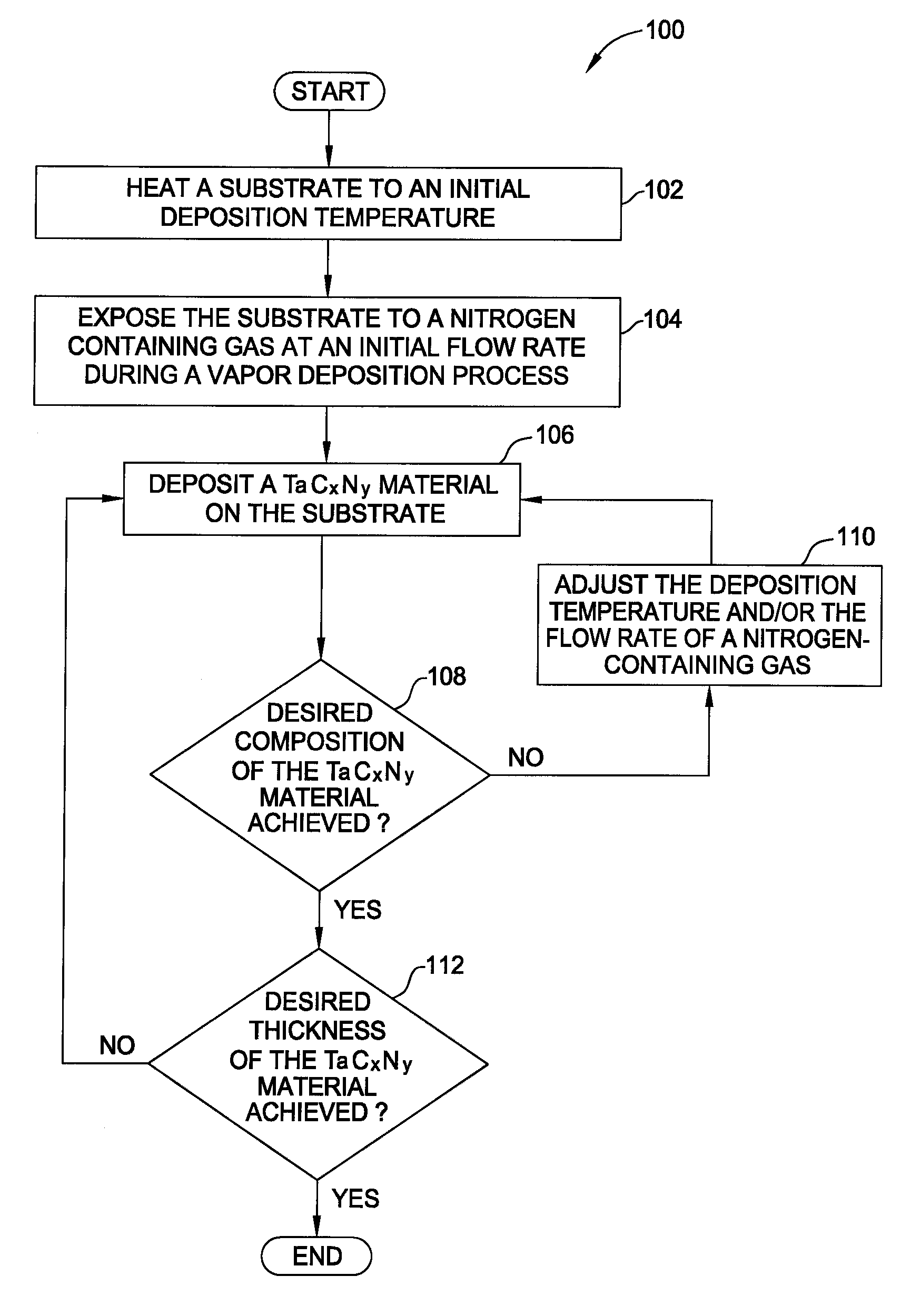
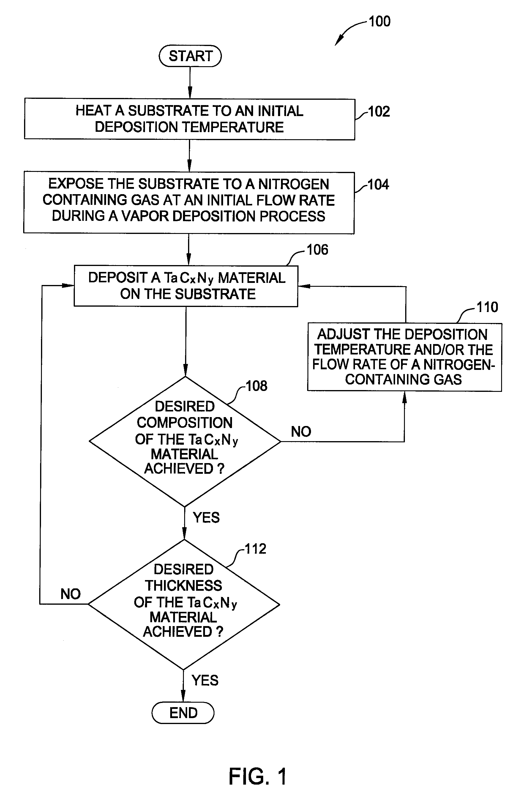
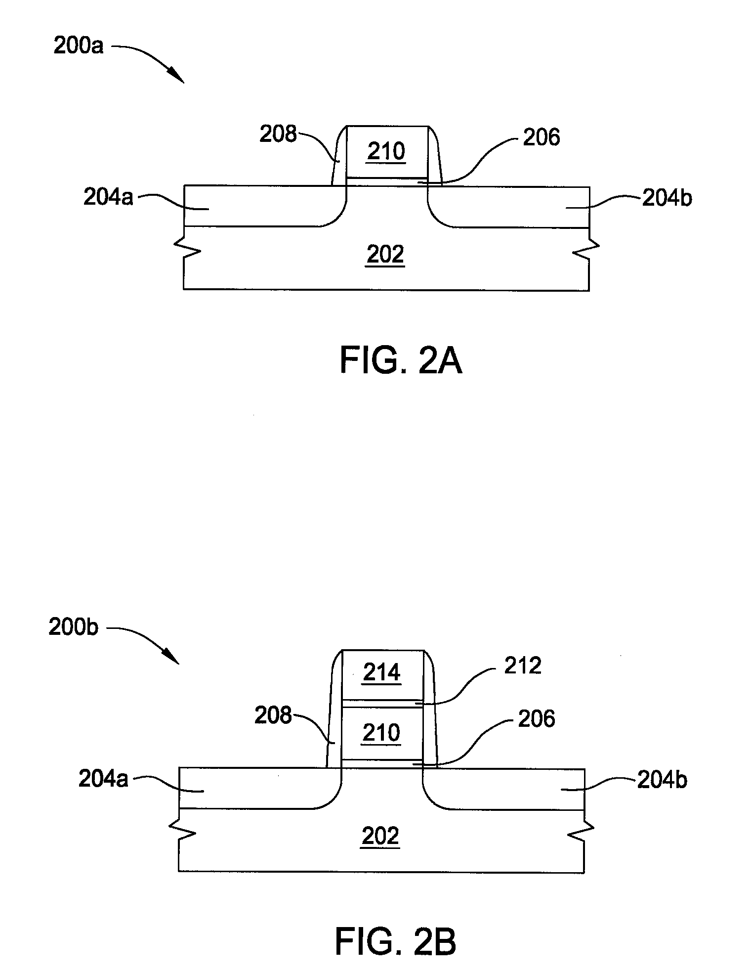
Vapor deposition processes for tantalum carbide nitride materials
a technology of tantalum carbide nitride and vapor deposition process, which is applied in the direction of chemical vapor deposition coating, coating, metallic material coating process, etc., can solve the problems of lacked accessible or tunable electronic properties of materials used for gate electrodes, dielectric layers to become conductive, and tantalum materials have only been scarcely used for metal gate electrode formation
- Summary
- Abstract
- Description
- Claims
- Application Information
AI Technical Summary
Benefits of technology
Problems solved by technology
Method used
Image

Examples
example 1
[0058]A tantalum carbide nitride material was deposited on a substrate by a thermal decomposition process by heating the substrate and the substrate pedestal to a temperature of about 425° C. The substrate was exposed to a tantalum precursor gas at a flow rate of about 500 sccm, of which, contained about 100 sccm of TBTEMT and about 400 sccm of argon carrier gas. The substrate was not exposed to a nitrogen-containing gas, such as ammonia. The tantalum carbide nitride material was deposited on the substrate to a final thickness of about 200 Å. The composition analysis of the tantalum carbide nitride material provided the respective atomic ratios of tantalum, carbon, and nitrogen to be 1.00:0.75:0.31. The XPS analysis of the tantalum carbide nitride material revealed the two different binding sites for carbon, indicative to the interstitial carbon and the elemental carbon. An interstitial / elemental carbon ratio was deduced from the XPS spectra. Therefore, the tant...
example 2
[0059]A tantalum carbide nitride material was deposited on a substrate by a thermal decomposition process by heating the substrate and the substrate pedestal to a temperature of about 475° C. The substrate was exposed to a tantalum precursor gas at a flow rate of about 500 sccm, of which, contained about 100 sccm of TBTEMT and about 400 sccm of argon carrier gas. The substrate was not exposed to a nitrogen-containing gas, such as ammonia. The tantalum carbide nitride material was deposited on the substrate to a final thickness of about 200 Å. The composition analysis of the tantalum carbide nitride material provided the respective atomic ratios of tantalum, carbon, and nitrogen to be 1.00:0.88:0.38. The tantalum carbide nitride material had an interstitial / elemental carbon ratio of about 2.44 per XPS analysis.
example 3
[0060]A tantalum carbide nitride material was deposited on a substrate by a thermal decomposition process by heating the substrate and the substrate pedestal to a temperature of about 495° C. The substrate was exposed to a tantalum precursor gas at a flow rate of about 500 sccm, of which, contained about 100 sccm of TBTEMT and about 400 sccm of argon carrier gas. The substrate was not exposed to a nitrogen-containing gas, such as ammonia. The tantalum carbide nitride material was deposited on the substrate to a final thickness of about 200 Å. The composition analysis of the tantalum carbide nitride material provided the respective atomic ratios of tantalum, carbon, and nitrogen to be 1.00:0.88:0.38. The tantalum carbide nitride material had an interstitial / elemental carbon ratio of about 3.65 per XPS analysis.
PUM
| Property | Measurement | Unit |
|---|---|---|
| temperature | aaaaa | aaaaa |
| size | aaaaa | aaaaa |
| temperature | aaaaa | aaaaa |
Abstract
Description
Claims
Application Information