

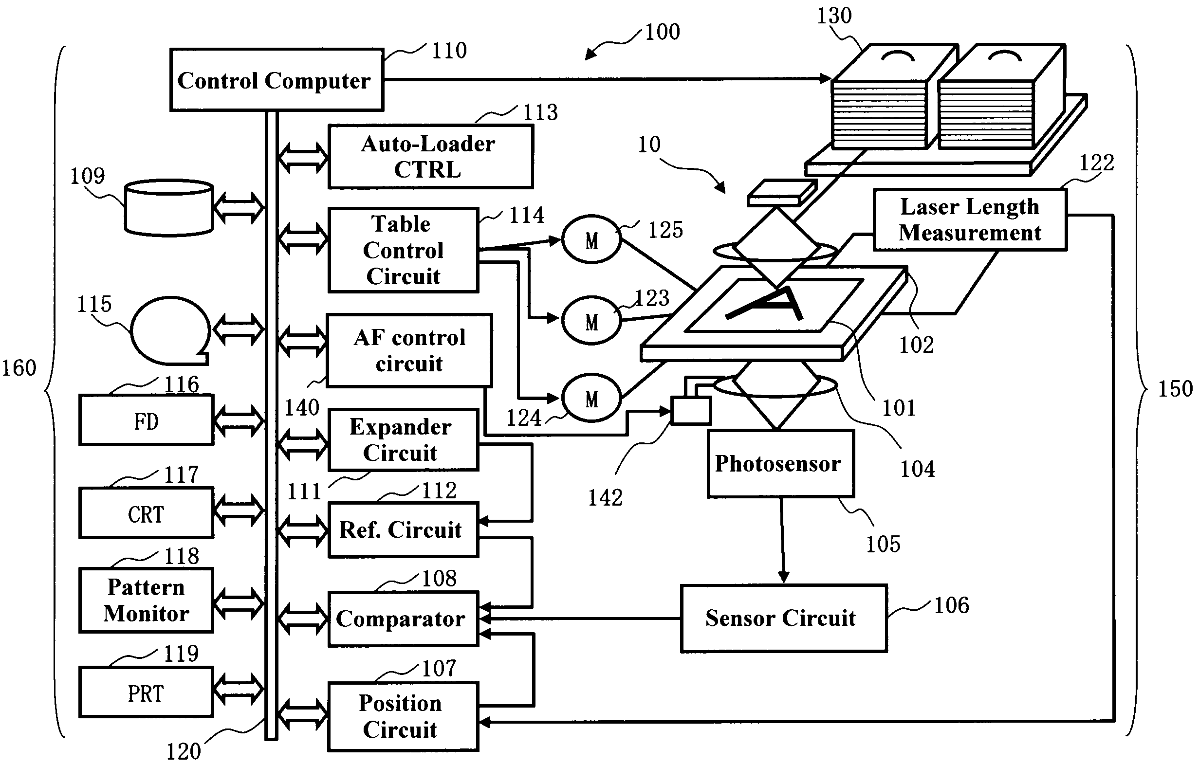
Beam irradiation apparatus with deep ultraviolet light emission device for lithographic pattern inspection system
a technology of ultraviolet light and lithographic pattern, which is applied in the direction of optical radiation measurement, fluorescence/phosphorescence, spectrometry/spectrometry/monochromator, etc., can solve the problem that the yield improvement cannot catch up the rapid growth of microfabrication of ulsi chips, and the feature size and circuit line width of semiconductor circuit elements are not easily noticeable, so as to reduce the degradation and deterioration of optical components used, suppress the deterioration of optical components
- Summary
- Abstract
- Description
- Claims
- Application Information
AI Technical Summary
Benefits of technology
Problems solved by technology
Method used
Image

Examples
Embodiment Construction
Illumination Apparatus
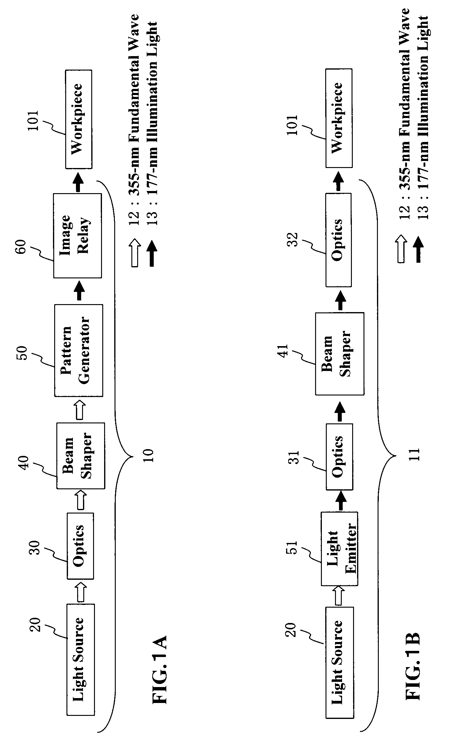
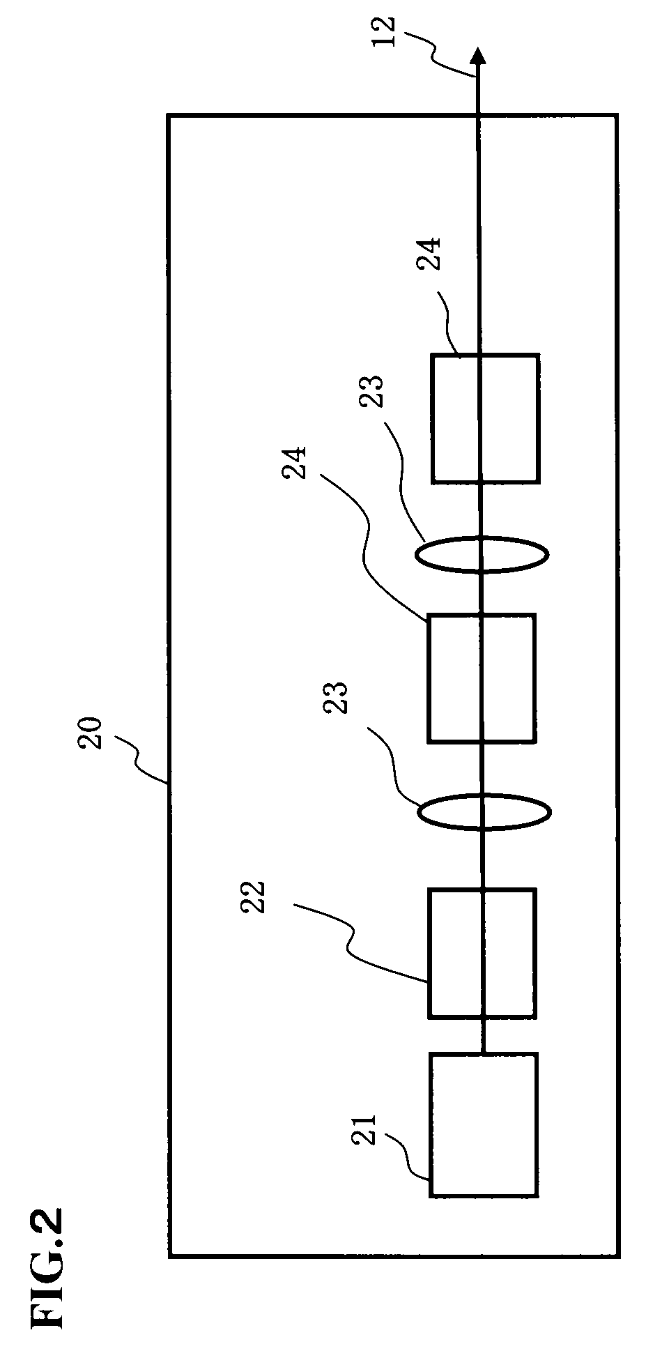
[0023]An illumination beam irradiation apparatus in accordance with one preferred embodiment of this invention is shown in FIG. 1A in block diagram form. In FIG. 1A, the illumination apparatus is designated by reference numeral 10. This illumination apparatus 10 is generally made up of a light source 20, optical system 30, beam-shaping unit 40, optical pattern generation unit 50, and image relay unit 60. The light source 20 is for yielding a fundamental wave 12 with a wavelength of 355nm as an example. The fundamental wave 12 emitted from light source 20 is transferred via the optics 30 to the beam shaper unit 40. This beam shaper is the one that performs beam-shaping of the fundamental wave 12 in a way such that this wave has a specific shape, such as a rectangle or square or else, resulting in production of the beam-shaped fundamental wave 12 having the specific shape. When this specifically shaped fundamental wave 12 enters the pattern generator 50, this uni...
PUM
| Property | Measurement | Unit |
|---|---|---|
| wavelength | aaaaa | aaaaa |
| wavelength | aaaaa | aaaaa |
| wavelength | aaaaa | aaaaa |
Abstract
Description
Claims
Application Information