Method of forming fine patterns and manufacturing semiconductor light emitting device using the same

a technology of semiconductor light emitting devices and fine patterns, which is applied in the direction of semiconductor devices, decorative arts, electrical equipment, etc., can solve the problems of limited light extraction efficiency, easy deterioration of semiconductor surface properties, and limitations of the etching process used in this patterning process to form fine patterns on a semiconductor surface. , to achieve the effect of minimizing the damage area

Active Publication Date: 2009-04-02
SAMSUNG ELECTRONICS CO LTD
View PDF10 Cites 62 Cited by
  • Summary
  • Abstract
  • Description
  • Claims
  • Application Information

AI Technical Summary

Benefits of technology

[0014]An aspect of the present invention provides a method of forming fine patterns, which can minimize a damaged area resulting from dry etching by using a horizontal etching characteristic of a {0001} c-plane hexagonal semiconductor crystal after the dry etching.
[0015]An aspect of the present invention also provides a method of manufacturing a semiconductor light emitting device having fine patterns, which has improved optical output by using the method of forming fine patterns.
[0021]The pattern of the mask may include a plurality of fine holes, and the second fine pattern may include a plurality of hexagonal fine holes. An inner wall of the hole may have a crystal plane that is varied over time of wet etching, which is a secondary etching process. The forming a second fine pattern may include performing wet-etching such that the sidewall of the second fine pattern has an m-plane component and an s-plane component. Also, by continuing the wet etching, an inner sidewall of the hole may include an r-plane component, which is more stable and can provide a lower coverage.
[0024]According to another aspect of the present invention, there is provided a method of manufacturing a semiconductor light emitting device, which can be advantageously applied to a phonic crystal structure required to have fine patterns or a structure using a surface plasmon resonance principle.
[0026]The second fine pattern formed at the second conductivity type semiconductor layer may serve as a photonic crystal structure that improves light extraction efficiency by attenuating a total reflection effect caused by a low refractive index of the ambient air or a sealant when light generated at the active layer is extracted to the outside through a surface of the p-type nitride semiconductor layer.

Problems solved by technology

In the case of a nitride semiconductor light emitting device, light-extraction efficiency is limited due to a difference in a refractive index between the outside and a nitride semiconductor.
However, an etching process used in this patterning process has limitations in forming fine patterns on a semiconductor surface.
The limitations vary according to an etching method being used.
However, the dry etching has limitations in that properties of a semiconductor surface easily deteriorate due to a physical bombardment with ions or neutral atoms during the dry etching.
Even if a thin film of a material, which is not p-type GaN, is deposited on a p-type GaN layer and then the thin film is patterned using dry etching, it is difficult to prevent damage to the p-type GaN layer placed at a portion where the thin film is removed.
In the nitride semiconductor light emitting device damaged by the dry etching, a current begins to flow from a low voltage.
However, this current is not the one that is generated by the normal carrier recombination but a leakage current that generates almost no light.
For this reason, using general post-processing cannot contribute to recovering the damaged crystal.
The conductivity type conversion becomes a fatal defect in a p-n junction diode.
However, the wet etching also has limitations in that a specific plane (e.g., a c-plane) of a nitride single crystal is not etched almost at all, and precise patterning is difficult to achieve.

Method used


Image

  • Method of forming fine patterns and manufacturing semiconductor light emitting device using the same
  • Method of forming fine patterns and manufacturing semiconductor light emitting device using the same
  • Method of forming fine patterns and manufacturing semiconductor light emitting device using the same

Examples


embodiment 1a

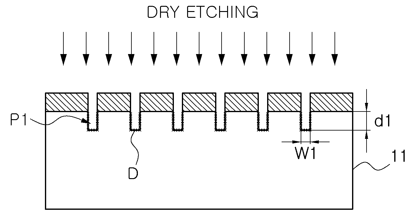
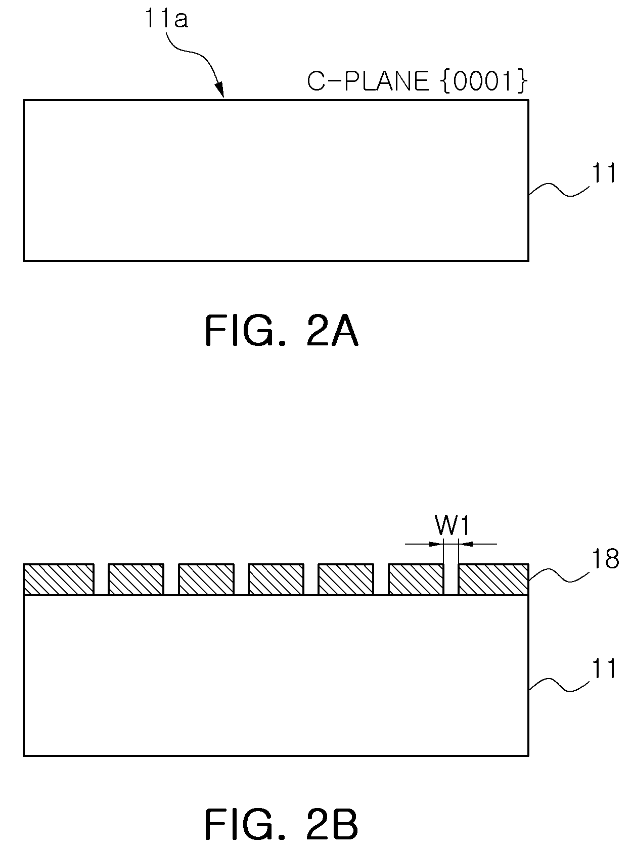
[0073]According to the current embodiment, a mask having line patterns formed in a orientation and arranged in a orientation is formed on a c-plane GaN semiconductor crystal. A period of the line patterns is set to about 0.6 μm. Thereafter, dry etching is performed up to a depth of about 0.1 μm, and then the mask is removed (see FIG. 3A).

[0074]Thereafter, wet etching using a 4M KOH aqueous solution is performed at about 100° C. for about 10 minutes, then an observation is made using a scanning electron microscope, and then the wet etching is further performed for about 20 minutes (total 30 minutes).

[0075]As a result of the wet etching performed for about ten minutes, an initial sidewall which is somewhat inclined becomes a vertical sidewall as shown in FIG. 3B. Since the sidewall becomes a {1-100} plane, which is a relatively stable crystal plane of GaN, i.e., an m-plane, the sidewall is no longer etched during the additional wet etching for about 20 minutes. Of course, a bottom s...

embodiment 1b

[0077]According to this embodiment, similarly to the embodiment 1A, a mask having a plurality of line patterns (period: about 0.6 μm) is formed on a c-plane GaN semiconductor crystal. The difference there is a formation orientation and an arrangement orientation thereof. That is, according to the current embodiment, a plurality of line patterns are formed in a orientation and arranged in a orientation. Thereafter, dry etching is performed up to a depth of about 0.1 μm, and then the mask is removed (see FIG. 4A).

[0078]Thereafter, wet etching using a 4M KOH aqueous solution is performed at a temperature of about 100° C. for about 10 minutes, and a resulting structure is observed using an SEM (see FIG. 4B). Thereafter, the wet etching is performed thereon for about 20 minutes (total 30 minutes) and a resulting structure is observed using the SEM (see FIG. 4C). Thereafter, the wet etching is performed additionally for about 20 minutes (total 50 minutes) and a resulting structure is ob...

embodiment 1c

[0084]Unlike the previous embodiments 1A and 1B, the current embodiment employs three-dimensional patterns. A plurality of circular mask patterns each having a size of about 0.3 μm are formed on a c-plane GaN semiconductor crystal. The plurality of circular mask patterns are arranged vertically and horizontally at a period of about 0.6 μm.

[0085]Thereafter, dry etching is performed up to a depth of about 0.1 μm, and then the mask is removed. Thereafter, wet etching using a 4M KOH aqueous solution is performed at about 100° C. for about 10 minutes and then a resulting structure is captured by using an SEM. As shown in FIG. 5, it can be seen that a three-dimension pattern such as a pillar structure (diameter: about 130 nm) is formed.


PUM

PropertyMeasurementUnit
thicknessaaaaaaaaaa
sharp angleaaaaaaaaaa
depthaaaaaaaaaa

Abstract

A method of forming a fine pattern begins with providing a c-plane hexagonal semiconductor crystal. A mask having a predetermined pattern is formed on the semiconductor crystal. The semiconductor crystal is dry-etched by using the mask to form a first fine pattern on the semiconductor crystal. The semiconductor crystal including the first fine pattern is wet-etched to expand the first fine pattern in a horizontal direction to form a second fine pattern. The second fine pattern obtained in the wet-etching the semiconductor crystal has a bottom surface and a sidewall that have unique crystal planes, respectively. The present fine-pattern forming process can be advantageously applied to a semiconductor light emitting device, particularly, to a phonic crystal structure required to have fine patterns or a structure using a surface plasmon resonance principle.

Description

CROSS-REFERENCE TO RELATED APPLICATIONS[0001]This application claims the priority of Korean Patent Application Nos. 2007-98320 filed on Sep. 28, 2007 and 2008-86063 filed on Sep. 1, 2008 in the Korean Intellectual Property Office, the disclosure of which is incorporated herein by reference.BACKGROUND OF THE INVENTION[0002]1. Field of the Invention[0003]The present invention relates to a fine-pattern forming process, and more particularly, to a process for manufacturing a semiconductor light emitting device including the fine patterns to improve light efficiency.[0004]2. Description of the Related Art[0005]Various semiconductor devices are being fabricated, such as light emitting diodes, laser diodes, photodiodes and transistors based on semiconductors.[0006]For specific functions, the semiconductor device may be required to have fine patterns such as periodic / non-periodic patterns at a predetermined region. Such fine patterns may be formed by etching a semiconductor surface using a ...

Claims


Application Information

Patent Timeline
Patent Type & Authority Applications(United States)
IPC IPC(8): H01L21/302H01L33/06H01L33/10H01L33/16H01L33/32H01L33/42
CPCH01L21/30617H01L21/30621H01L33/382H01L33/20H01L33/22H01L21/3083
Inventor LEE, JONG HOPARK, MOO YOUNHWANG, SOO RYONGJUNG, IL HYUNGLEE, GWAN SUKIM, JIN HA
Owner SAMSUNG ELECTRONICS CO LTD
Why Eureka
Try Eureka