Semiconductor device

a semiconductor and high-withstand technology, applied in the field of semiconductor devices, can solve the problems of difficult to form sufficient p-type regions, difficult to achieve the wide bandgap semiconductor, and difficult to form p-type regions by ion injection method, so as to achieve convenient production, improve reliability, and avoid high controllability.

Active Publication Date: 2009-05-07
FUJI ELECTRIC CO LTD
View PDF2 Cites 48 Cited by
  • Summary
  • Abstract
  • Description
  • Claims
  • Application Information

AI Technical Summary

Benefits of technology

[0010]According to the invention, the semiconductor device can be easily produced to improve reliability because the invention can dispense with high controllability for forming an inclined surface of a bevel structure. Since the insulating film in the trench in the peripheral voltage withstanding structure portion absorbs a large part of a voltage applied between a source and a drain, the length of the peripheral voltage withstanding structure portion can be shortened so as to be approximately equal to the width of the trench in the peripheral voltage withstanding structure portion. Since the second semiconductor layer of the first conductivity type in the peripheral voltage withstanding structure portion serves as a stopper of a depletion layer, it is unnecessary to provide a depletion layer stretching prevention region (region equivalent to the n+ region in the background art) in an element edge portion. When the fourth semiconductor layer of the second conductivity type is provided along the bottom of the trench, the depletion later can be spread stably to improve the element withstand voltage.
[0011]In the semiconductor device according to the invention, there is an effect that the semiconductor device can be produced easily. There is another effect that the semiconductor device is excellent in long-term reliability. There is a further effect that a peripheral voltage withstanding structure portion of the semiconductor device can be made short.

Problems solved by technology

On the other hand, SiC or GaN has a disadvantage that it is very difficult to form P-type regions by an ion injection method.
Although it has been reported that SiC turned p type when aluminum (Al) or gallium (Ga) ions were injected into SiC at a high temperature, it is impossible to form sufficient p-type regions because resistance is very high.
That is, it is difficult for the wide bandgap semiconductor to form p-type regions selectively in an n-type substrate.
For this reason, it is very difficult to provide a guard ring in a peripheral voltage withstanding structure portion surrounding an active region portion in which a drift current flows.
The peripheral voltage withstanding structure disclosed in JP-A-2002-185015, however, has the following problems.
Firstly, since the element withstand voltage depends on the taper angle of the inclined surface, high controllability is required of the dry etching.
Secondly, it is necessary to prevent the inclined surface and the surface of the n− layer from being damaged by the dry etching.
Because of these requirements, it is difficult to produce a semiconductor device having a desired element withstand voltage at a good yield rate.
Moreover, it is difficult to obtain sufficiently high reliability for a long term.

Method used


Image

  • Semiconductor device
  • Semiconductor device
  • Semiconductor device

Examples


embodiment 1

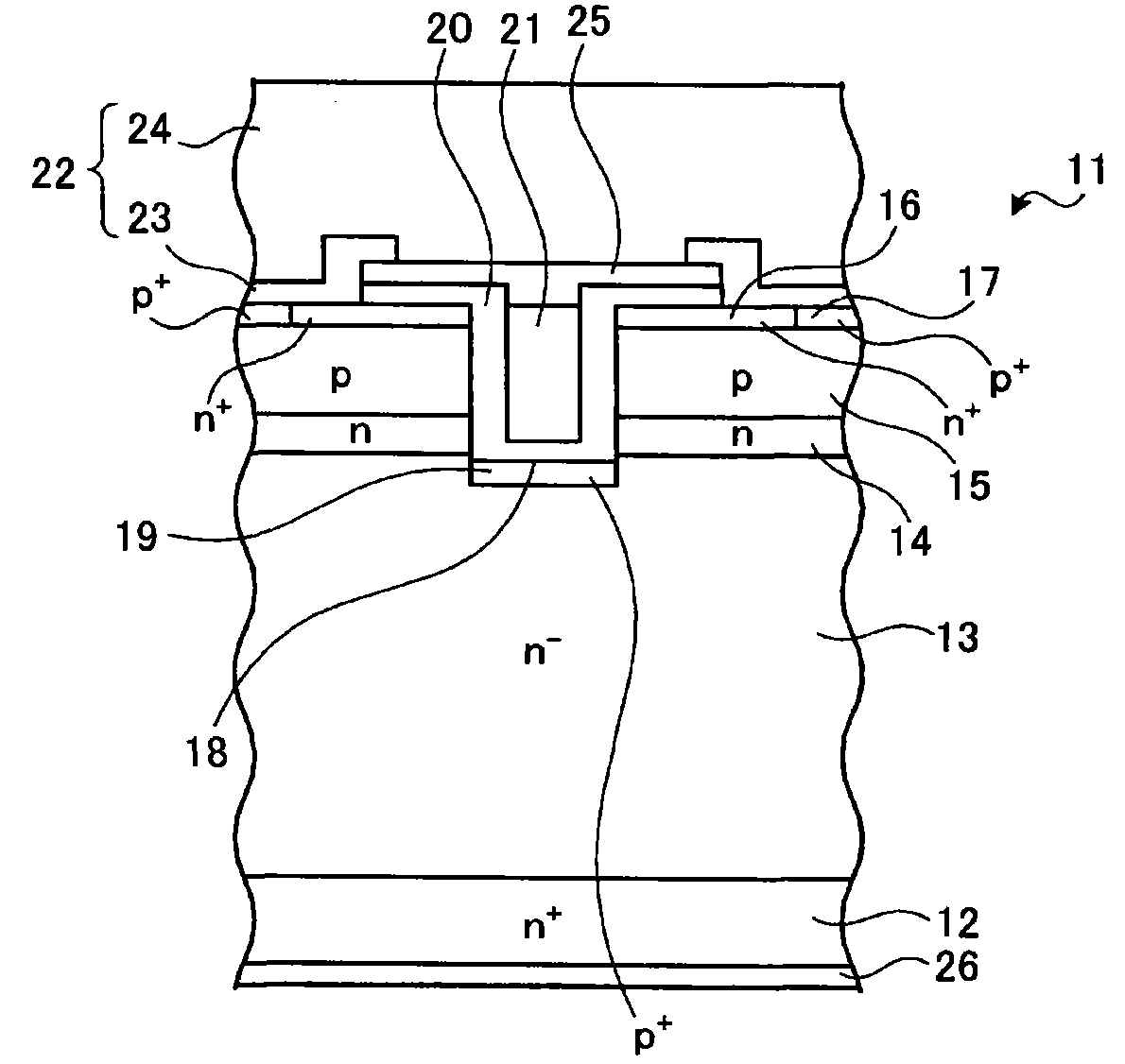
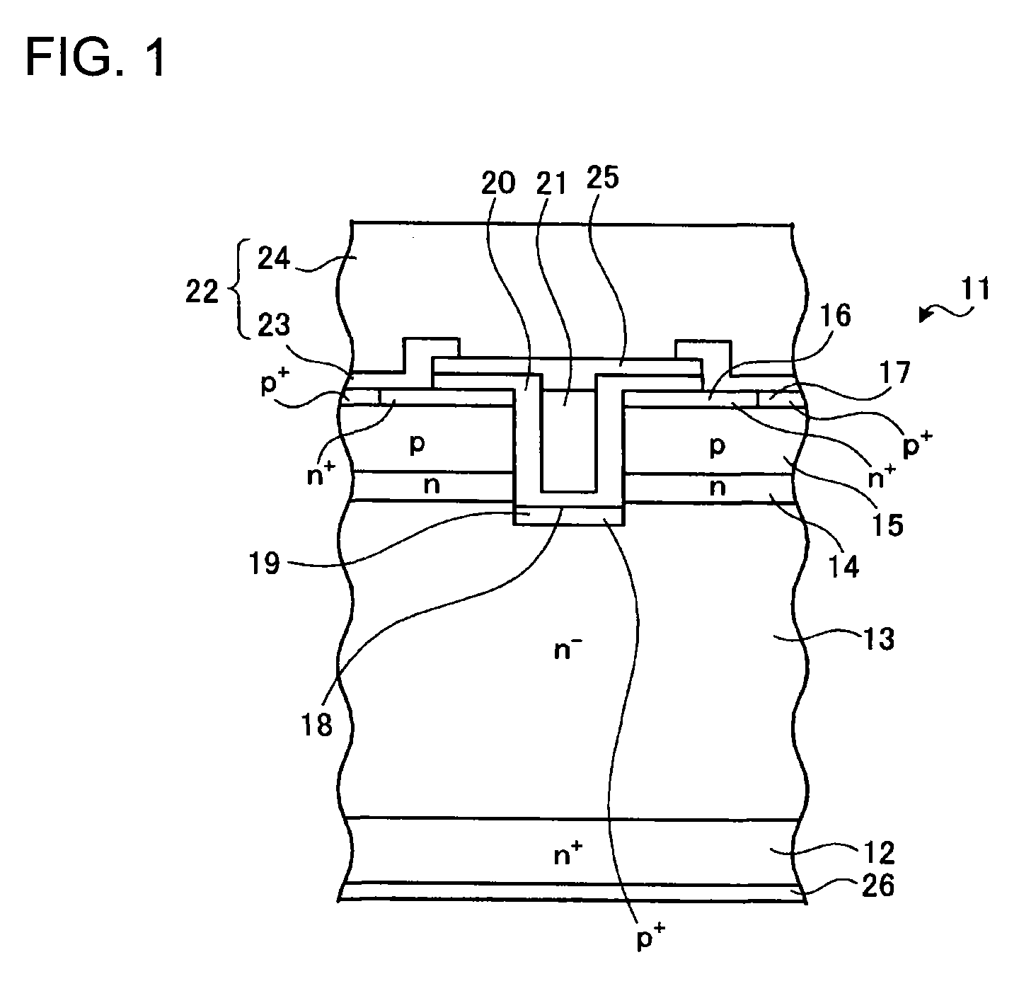
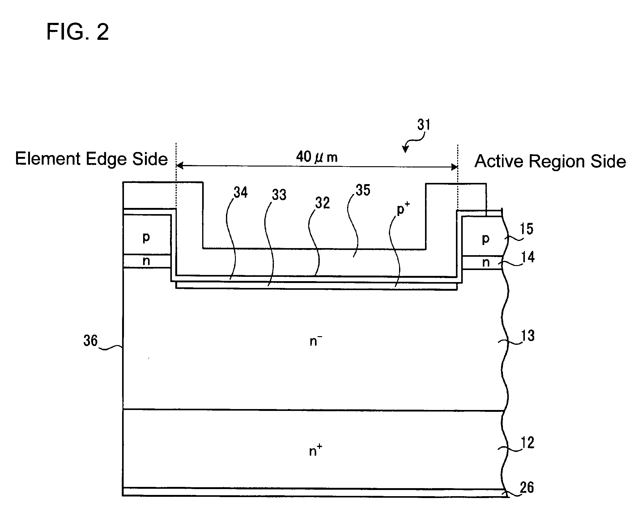
[0027]FIGS. 1 and 2 are sectional views showing respective configurations of an active region portion and a peripheral voltage withstanding structure portion in a semiconductor device according to a first embodiment of the invention. Description will be made on the case where a trench gate MOSFET of 1200V withstand voltage class is taken as an example though the semiconductor device is not particularly limited to the trench gate MOSFET. The active region portion and the peripheral voltage withstanding structure portion are formed in one and the same semiconductor substrate so that the outside of the active region portion is surrounded by the peripheral voltage withstanding structure portion. The semiconductor device is produced from SiC. A first conductivity type is an n type, and a second conductivity type is a p type.

[0028]As shown in FIG. 1, in the active region portion 11, an n− SiC layer 13 is provided on an n+ SiC layer 12. For example, the n+ SiC layer 12 contains about 2×101...

embodiment 2

[0051]FIGS. 11 and 12 are sectional views showing the respective configurations of an active region portion and a peripheral voltage withstanding structure portion in a semiconductor device according to the second embodiment. Description will be made on the case where a trench gate type IGBT of a 1200V withstand voltage class is taken as an example though the semiconductor device is not particularly limited thereto. The active region portion and the peripheral voltage withstanding structure portion are formed in one and the same semiconductor substrate. The semiconductor device is produced from SiC. The first conductivity type is a p type and the second conductivity type is an n type.

[0052]Generally, the IGBT using SiC is of a p channel type. This is because the resistance of a p-type SiC substrate is so high that an n-type IGBT produced by use of this substrate is said to be impractical due to a very large voltage drop in the substrate. Therefore, the second embodiment will be desc...

embodiment 3

[0065]In the third embodiment, GaN is used as a semiconductor material in place of SiC used in the first embodiment. The configuration of the MOSFET is the same as in the first embodiment except that a different semiconductor material is used. Accordingly, with respect to the description of the configuration and producing process in the third embodiment, SiC in the description of the first embodiment can be replaced by GaN.

[0066]Incidentally, a substrate, for example, containing about 2×1018 cm−3 of silicon is prepared as an n-type GaN semiconductor substrate which serves as an n+ GaN layer (corresponding to the n+ SiC layer 12 in the first embodiment). The impurity to be imported into a p GaN layer, a p+ contact region and a p+GaN region (corresponding to the p SiC layer 15, the p+ contact region 17 and the p+ SiC region 19 respectively in Embodiment 1) is changed to magnesium.

[0067]Description will be made about a result of comparison in the length of the peripheral voltage withst...


PUM


Abstract

A semiconductor device includes a peripheral voltage withstanding structure, which includes an n SiC layer, an n SiC layer and a p SiC layer are provided successively on an n+ SiC layer. A trench is formed in the peripheral voltage withstanding structure portion so that the trench passes through the p SiC layer 15 and the n SiC layer 14 and reaches the n SiC layer. This trench is wider than a trench having a trench gate structure in the active region portion. A p+ SiC region is provided along a bottom of the trench so as to be located under the trench. A sidewall and the bottom of the trench are covered with an oxide film and an insulating film having a total thickness not smaller than 1.1 μm. The oxide film and insulating film absorb a large part of a voltage applied between a source and a drain.

Description

BACKGROUND OF THE INVENTION[0001]The present invention relates to a semiconductor device and particularly relates to a high withstand voltage semiconductor device produced from a semiconductor material (hereinafter referred to wide bandgap semiconductor) having a wider bandgap than that of silicon.[0002]Wide bandgap semiconductors such as silicon carbide (hereinafter referred to as SiC), gallium nitride (hereinafter referred to as GaN), etc. have recently attracted a great deal of attention as semiconductor materials for power semiconductor devices. The wide bandgap semiconductors potentially break the characteristic limit of silicon which is a conventional semiconductor material. On the other hand, SiC or GaN has a disadvantage that it is very difficult to form P-type regions by an ion injection method. Although it has been reported that SiC turned p type when aluminum (Al) or gallium (Ga) ions were injected into SiC at a high temperature, it is impossible to form sufficient p-type...

Claims


Application Information

Patent Timeline
Patent Type & Authority Applications(United States)
IPC IPC(8): H01L29/24H01L29/78
CPCH01L29/0623H01L29/0638H01L29/0661H01L29/0878H01L29/1608H01L29/7813H01L29/45H01L29/66068H01L29/66734H01L29/7397H01L29/7811H01L29/2003
Inventor IWAMURO, NORIYUKI
Owner FUJI ELECTRIC CO LTD
Why Eureka
Try Eureka