Silicon carbide semiconductor device and related manufacturing method

a technology of silicon carbide and semiconductor devices, applied in semiconductor devices, electrical apparatus, transistors, etc., can solve problems such as difficulty in high voltage, and achieve the effects of improving effect, low resistance, and reducing the electric field of an area beneath the trench

Active Publication Date: 2009-05-07
DENSO CORP
View PDF5 Cites 102 Cited by
  • Summary
  • Abstract
  • Description
  • Claims
  • Application Information

AI Technical Summary

Benefits of technology

[0013]The SiC semiconductor device may preferably further include, for instance, second electrically conductive type contact regions, spaced in placement from the trench so as to sandwich the source region to allow the base regions to be electrically connected to the first electrode, each of which has a higher concentration than that of the base region. In this case, the deep layer is placed beneath the contact region to be unitarily formed with the contact region. The deep layer has a second electrically conductive type impurity concentration ranging from, for instance, 1.0×10¹⁷/cm3 to 1.0×10²⁰/cm3. Further, the deep layer may be preferably arranged to have a depth of, for instance, 1.5 to 3.5 μm from a surface of the base region.
[0014]The SiC semiconductor device may preferably further comprise a second electrically conductive type reserve layer, formed on the drift layer in an area below the trench and the deep layer, which has a lower concentration than that of the deep layer.
[0015]With such a reserve layer being provided, an electric field of an area beneath the trench can be

Problems solved by technology

This allows a depletion layer, present in a PN junction between the deep layer and the drift layer, to remarkably extend to the drift l

Method used


Image

  • Silicon carbide semiconductor device and related manufacturing method
  • Silicon carbide semiconductor device and related manufacturing method
  • Silicon carbide semiconductor device and related manufacturing method

Examples


first embodiment

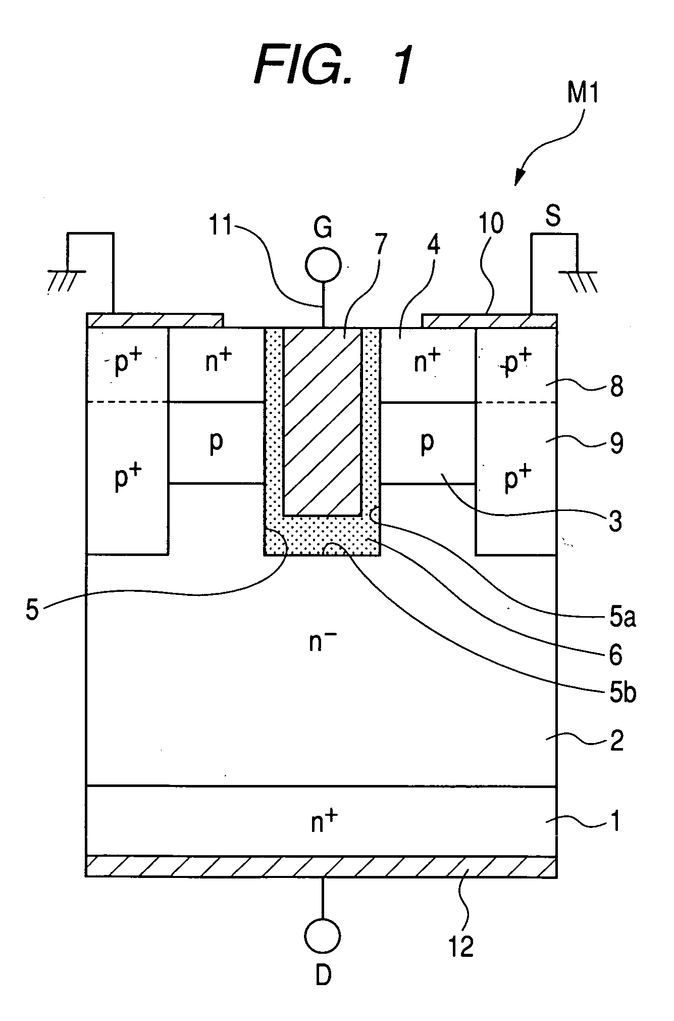
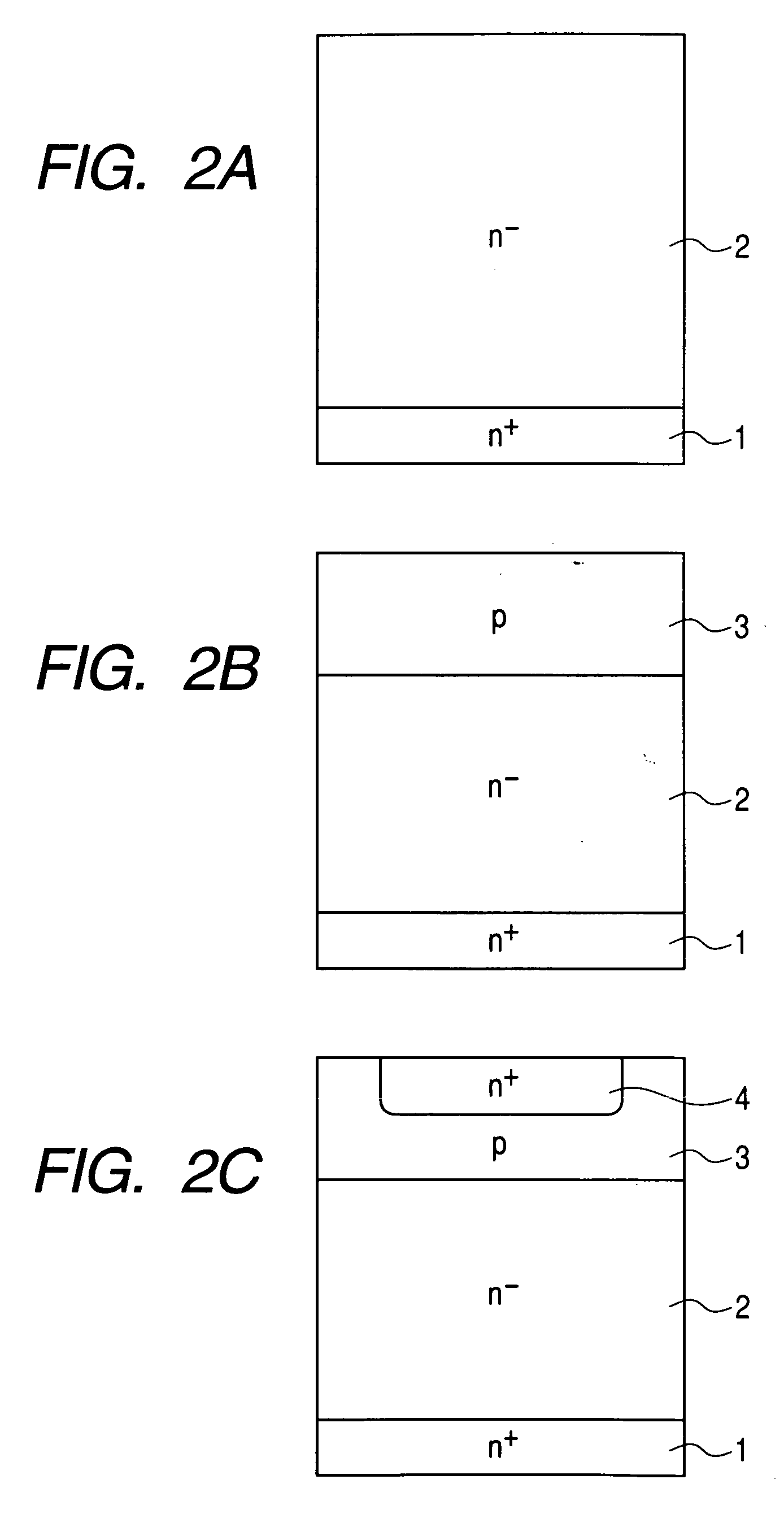
[0039]A silicon carbide (SiC) semiconductor device of a first embodiment according to the present invention will be described below in detail with reference to FIGS. 1 to 3. Here, a MOSFET of an inversion-type trench gate structure will be described as an element incorporated in the SiC semiconductor device.

[0040]FIG. 1 is a cross-sectional view of the MOSFET of such a trench gate structure of the present embodiment. Although FIG. 1 shows the MOSFET in terms of only one cell, it will be appreciated that the semiconductor device takes the form of a structure including a plurality of MOSFETs juxtaposed to each other with the same structures as that of the MOSFET shown in FIG. 1.

[0041]As shown in FIG. 1, the MOSFET M1 employs an n+-type substrate 1 as a semiconductor substrate, which has a surface laying on a (000-1) c-plane with a thickness of about 300 μm while containing a nitrogen (an n-type impurity) concentration of approximately 1.0×10¹⁹ / cm3. The n+-type substrate 1 has one surf...

second embodiment

[0067]A MOSFET M2 of an accumulation-type trench gate structure of a second embodiment according to the present invention will be described below with reference to FIG. 4. The MOSFET M2 of the present embodiment has the same fundamental structure as that of the MOSFET M1 of the first embodiment set forth above. Thus, the MOSFET of the present embodiment will be described below with a focus on points different from the MOSFET M1 of the first embodiment.

[0068]FIG. 4 is a cross-sectional view of the MOSFET M2 of the accumulation-type trench gate structure of the present embodiment. As will be clear from FIG. 4, the p-type base regions 3 are spaced from the sidewalls of the trench 5 each by a given distance to provide a structure with the n−-type drift layer 2 remaining in an n-type channel layer 30.

[0069]The MOSFET M2 of such an accumulation-type trench gate structure of the present embodiment will operate in a manner described below.

[0070]Under a condition before a gate voltage is app...

third embodiment

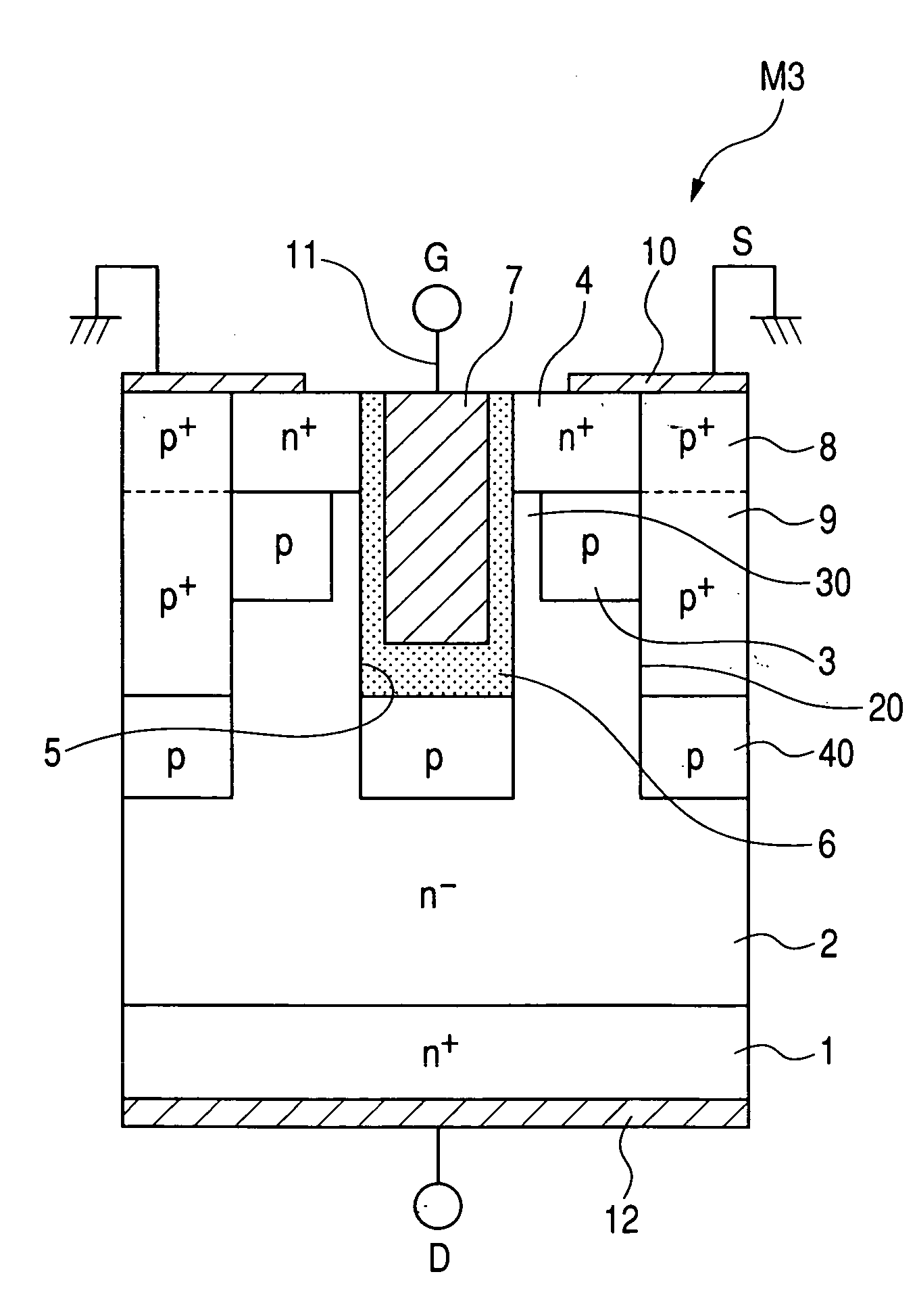
[0081]A MOSFET M3 of an accumulation-type trench gate structure of a third embodiment according to the present invention will be described below with reference to FIG. 7. The MOSFET M3 of the present embodiment differs from the MOSFET M2 of the trench gate structure of the second embodiment in respect of reserve layers being additionally provided. The MOSFET M3 of the present embodiment has the same fundamental structure as that of the MOSFET M2 of the second embodiment and, hence, description will be made with a focus on such a differing point.

[0082]FIG. 7 is a cross-sectional view of the MOSFET M3 of the accumulation-type trench gate structure of the present embodiment. As will be clear from FIG. 7, the MOSFET M3 of the present embodiment has areas, placed beneath the p+-type deep layers 9 at positions below the bottom wall of the trench layer 5, which have p-type reserve regions 40. Each of the p-type reserve regions 40 has a lower concentration than that of the p+-type deep laye...


PUM


Abstract

An SiC semiconductor device and a related manufacturing method are disclosed having a structure provided with a p+-type deep layer formed in a depth equal to or greater than that of a trench to cause a depletion layer between at a PN junction between the p+-type deep layer and an n-type drift layer to extend into the n-type drift layer in a remarkable length, making it difficult for a high voltage, resulting from an adverse affect arising from a drain voltage, to enter a gate oxide film. This results in a capability of minimizing an electric field concentration in the gate oxide film, i.e., an electric field concentration occurring at the gate oxide film at a bottom wall of the trench.

Description

CROSS REFERENCE TO RELATED APPLICATIONS[0001]This application is related to Japanese Patent Application No. 2007-288545, filed on Nov. 6, 2007, the content of which are hereby incorporated by reference.BACKGROUND OF THE INVENTION[0002]1. Technical Field of the Invention[0003]The present invention relates to silicon carbide semiconductor devices and, more particularly, to a silicon carbide semiconductor device (hereinafter referred to as “SiC”) having a trench gate, and a related manufacturing method.[0004]2. Description of the Related Art[0005]In recent years, a SiC has been getting a lot of attention as raw material for power devices with increased electric-field breakdown strength. Due to the SiC semiconductor device formed with increased electric-field breakdown strength, the SiC semiconductor device is able to controllably switch a flow of large electric current. Therefore, the SiC semiconductor device has been expected to have applications to a control of a motor of a hybrid ve...

Claims


Application Information

Patent Timeline
IPC IPC(8): H01L29/94H01L21/04H01L29/68
CPCH01L29/045H01L29/0619H01L29/0623H01L29/0634H01L29/0847H01L29/1095H01L29/7828H01L29/47H01L29/66068H01L29/7391H01L29/7397H01L29/7813H01L29/1608
Inventor SUZUKI, NAOHIROTAKEUCHI, YUUICHIENDO, TAKESHIOKUNO, EIICHIYAMAMOTO, TOSHIMASA
Owner DENSO CORP
Why Eureka
Try Eureka