Discrete time amplifier circuit and analog-digital converter

a technology of amplifier circuit and analog-digital converter, which is applied in the direction of amplifiers with semiconductor devices/discharge tubes, differential amplifiers, instruments, etc., can solve the problems of increasing current consumption, deteriorating characteristics of amplifier circuits, and increasing current consumption, so as to achieve low current consumption, simple circuit configuration, and high data transmission speed

Active Publication Date: 2009-05-07
SOCIONEXT INC
View PDF6 Cites 93 Cited by
  • Summary
  • Abstract
  • Description
  • Claims
  • Application Information

AI Technical Summary

Benefits of technology

[0019]For the purpose of simultaneously attaining high data transmission speed and low current consumption, the present invention is intended to provide a discrete time amplifier circuit having a simple circuit configuration, operating at double sampling timing and capable of shortening convergence time and to provide an AD converter incorporating this discrete time amplifier circuit.

Problems solved by technology

However, since common-mode feedback control (CMFB control) cannot be performed at double sampling timing in the conventional amplifier circuit configured as described above, the output common-mode voltage varies every half cycle, and there is a problem in which the characteristics of the amplifier circuit deteriorate.
However, the continuous time CMFB circuit is disadvantageous in that the circuit is complicated and that current consumption is increased since the circuit operates at all times. Furthermore, if the performance of the active elements used therein changes, the characteristics of the circuit change, and there is a problem in which the control range that can be used to ensure the credibility of the active elements used therein is restricted.
However, since the discrete time CMFB circuit performs sampling (single sampling) every cycle and cannot perform CMFB control at double sampling timing, there is a problem in which the output common-mode voltage varies every half cycle and the characteristics of the operational amplifier deteriorate.
Moreover, since the discrete time CMFB circuit performs feedback every cycle, there is a problem in which the initial pull-in period elapsing until the steady state is attained takes time.
19 cannot perform CMFB control at double sampling timing (circuit operation performed every half cycle) as described above, the output common-mode voltage varies every half cycle, and there is a problem in which the characteristics of the operational amplifier deteriorate.
Furthermore, the conventional continuous time CMFB circuit is disadvantageous in that the circuit is complicated and that current consumption is increased since the circuit operates at all times. Moreover, if the performance of the active elements used therein changes, the characteristics of the circuit change, and there is a problem in which the control range that can be used is restricted.
Still further, since the conventional discrete time CMFB circuit cannot perform CMFB control at double sampling timing, there is a problem in which the output common-mode voltage varies every half cycle and the characteristics of the operational amplifier deteriorate.
Moreover, since the conventional discrete time CMFB circuit performs feedback every cycle, there is a problem in which the so-called settling time becomes long, that is, the initial pull-in period elapsing until the steady state is attained takes time.

Method used


Image

  • Discrete time amplifier circuit and analog-digital converter
  • Discrete time amplifier circuit and analog-digital converter
  • Discrete time amplifier circuit and analog-digital converter

Examples


embodiment 1

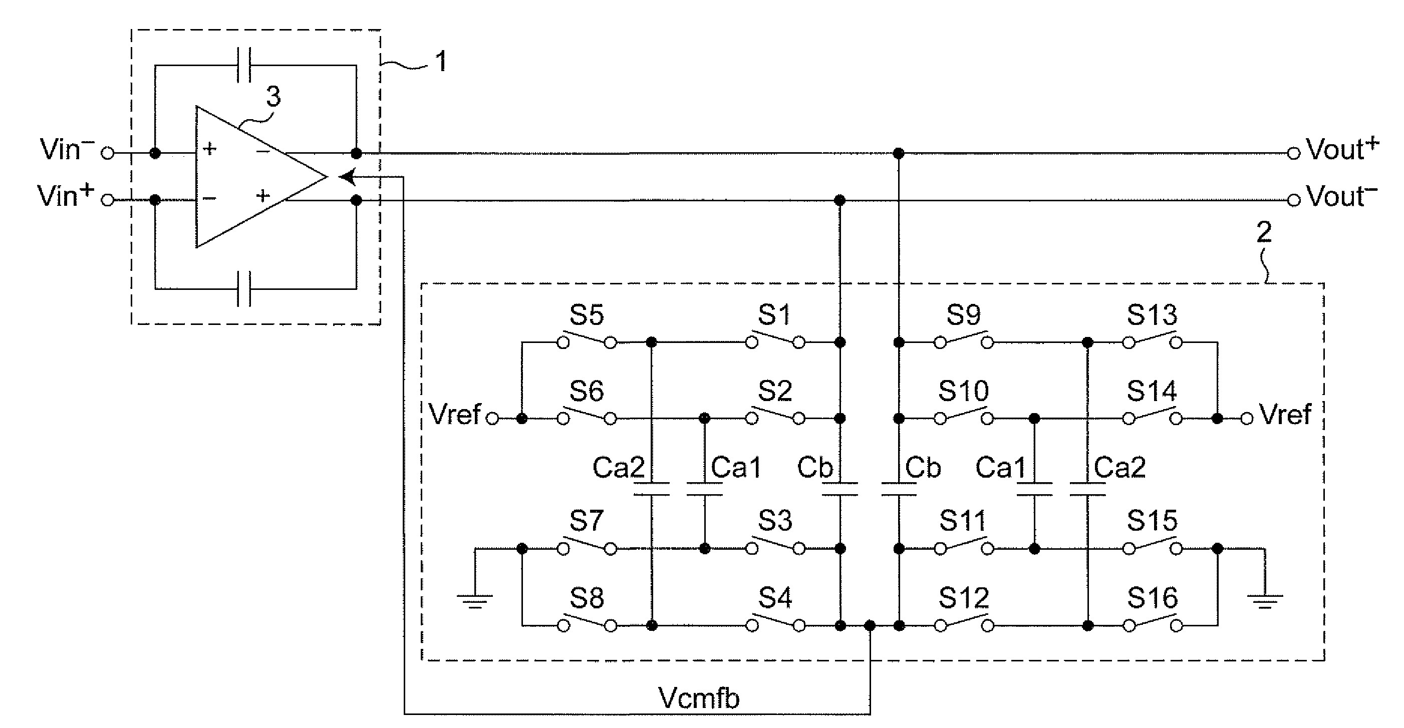
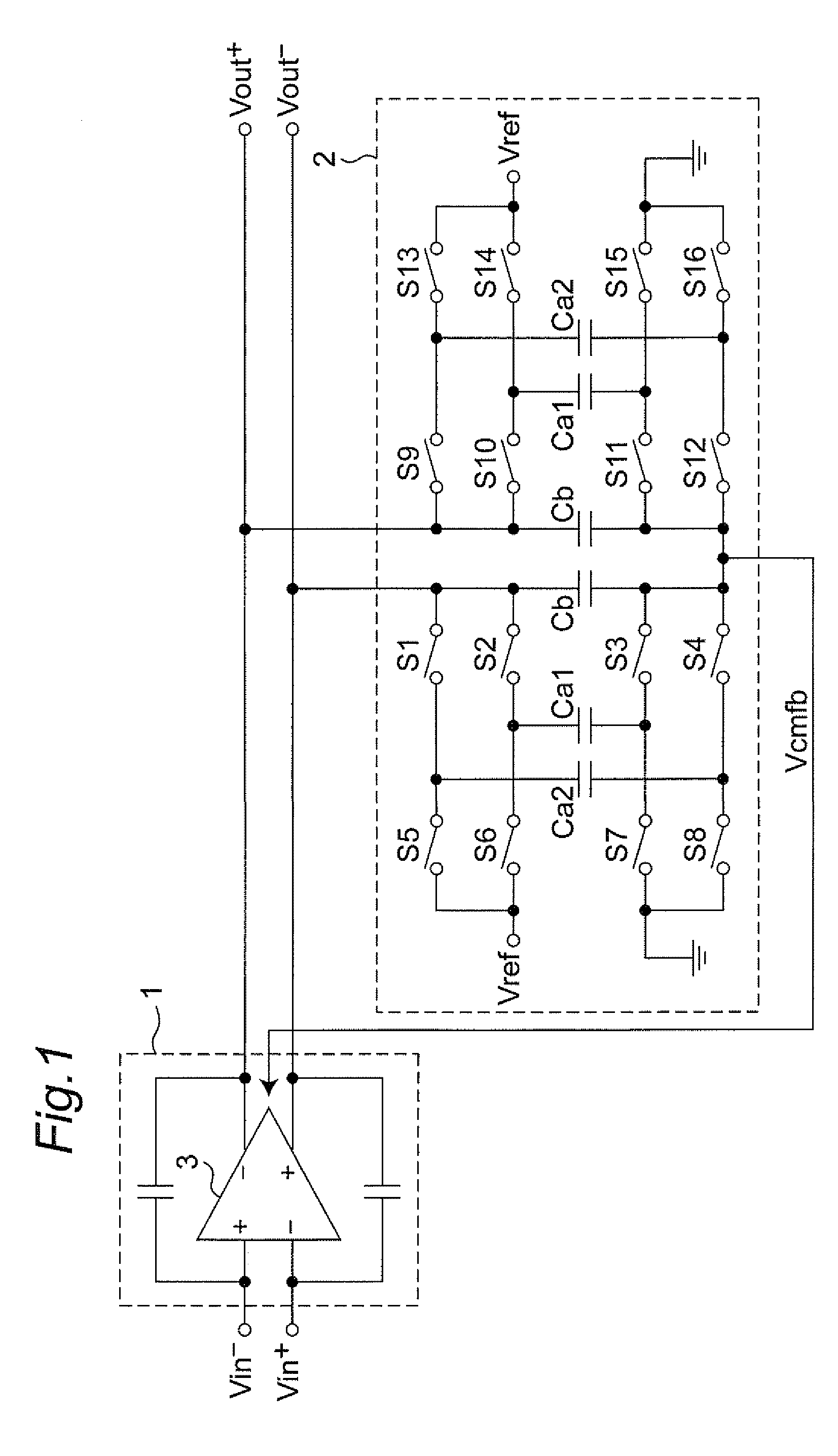
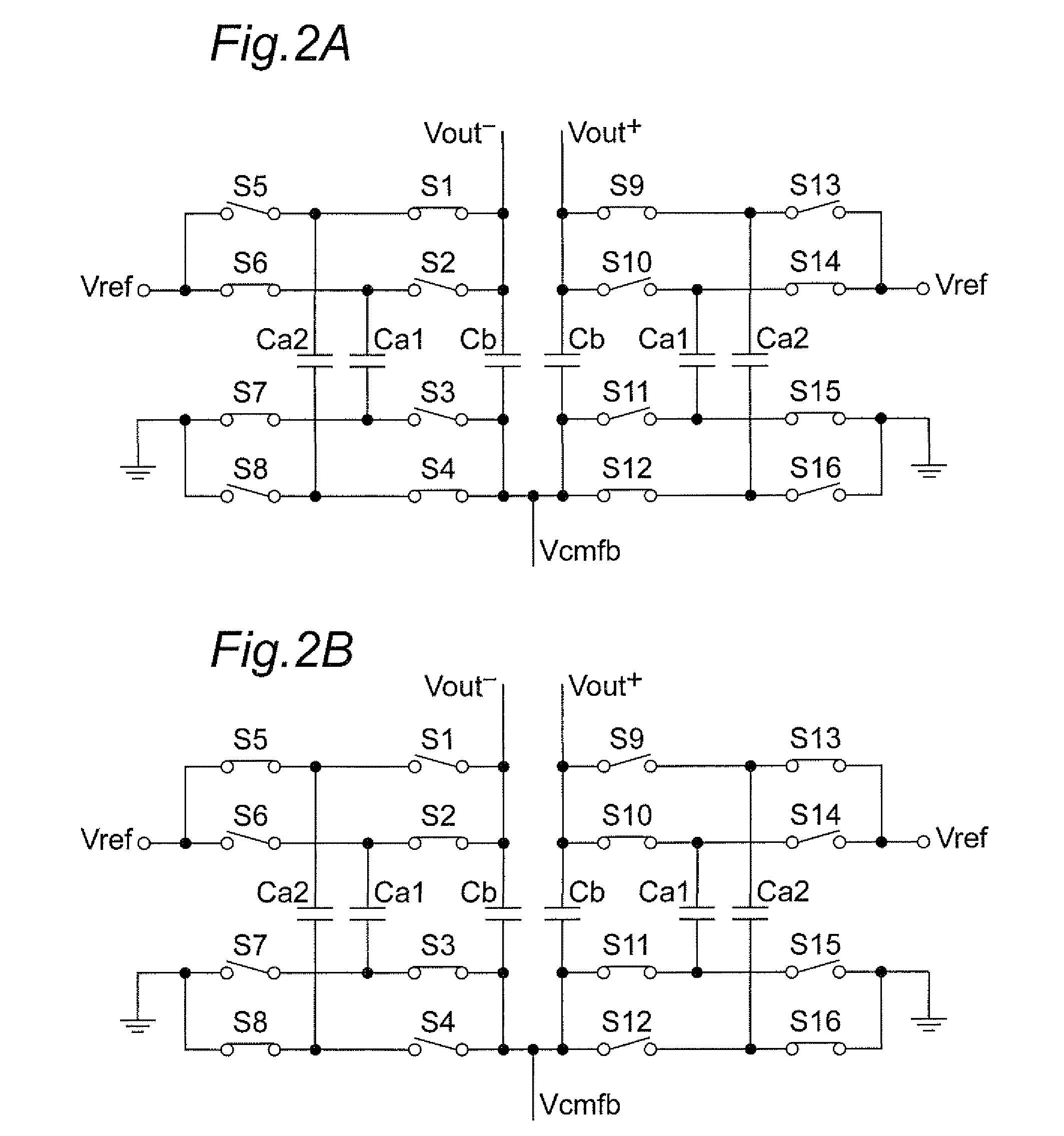
[0066]FIG. 1 is a circuit diagram showing a discrete time amplifier circuit having a discrete time common-mode feedback circuit according to Embodiment 1. As shown in FIG. 1, the discrete time amplifier circuit according to Embodiment 1 comprises a differential amplifier 1 for amplifying a differential signal and a discrete time common-mode feedback circuit (hereafter simply referred to as a CMFB circuit) 2 for controlling the output voltage (output common-mode voltage Vcmo) of the differential amplifier 1 to a reference voltage Vref.

[0067]The CMFB circuit 2 according to Embodiment 1 is equipped with multiple capacitors Ca1, Ca2 and Cb and multiple switches S1 to S16. The multiple capacitors of the CMFB circuit 2 include first sampling capacitors Ca1, second sampling capacitors Ca2 and hold capacitors Cb. The first sampling capacitor Ca1 and the second sampling capacitor Ca2 alternately sample a charge corresponding to the reference voltage Vref every ½ cycle. The hold capacitor Cb ...

embodiment 2

[0099]A discrete time amplifier circuit and an AD converter incorporating the discrete time amplifier circuit according to Embodiment 2 of the present invention will be described below referring to the accompanying drawings.

[0100]FIG. 10 is a circuit diagram showing a common-mode feedback circuit (hereafter simply referred to as a CMFB circuit) 20 in the discrete time amplifier circuit according to Embodiment 2 of the present invention. As shown in FIG. 10, the CMFB circuit 20 according to Embodiment 2 is provided with multiple sampling capacitors Ca1, Ca2, Ca3, . . . , Can, two hold capacitors Cb and multiple switches. The multiple switches are switches that connect the capacitors Ca1, Ca2, Ca3, . . . , Can to the input and output sides of the CMFB circuit 20 and switches that connect the capacitors to the side of the reference voltage (Vref). Furthermore, the hold capacitors Cb are connected to the input and output sides of the CMFB circuit 20 and further connected in parallel wit...

embodiment 3

[0109]A discrete time amplifier circuit and an AD converter incorporating the discrete time amplifier circuit according to Embodiment 3 of the present invention will be described below referring to the accompanying drawings.

[0110]FIG. 12 is a circuit diagram showing a common-mode feedback circuit (hereafter simply referred to as a CMFB circuit) 30 in the discrete time amplifier circuit according to Embodiment 3 of the present invention. As shown in FIG. 12, multiple hold capacitors serving as a common-mode feedback voltage generating circuit for generating and holding the common-mode feedback voltage are formed in the CMFB circuit 30. In other words, hold capacitors Cb1, Cb2, Cb3, . . . , Cbn are connected to the input and output terminals of the CMFB circuit 30 via switches Sw1, Sw2, Sw3, . . . , Swn, respectively. The capacitance values of the hold capacitors Cb1, Cb2, Cb3, . . . , Cbn are set at different values, and either one of the hold capacitors Cb1, Cb2, Cb3, . . . , Cbn ca...


PUM


Abstract

The present invention is intended to attain simplified circuit configuration and low current consumption in a discrete time amplifier circuit and an AD converter, to improve the convergence from the transient response state to the steady state of the amplifier circuit and to reduce noise and distortion owing to the variation in the output common-mode voltage. The discrete time amplifier circuit and the AD converter are provided with a switched-capacitor common-mode feedback (CMFB) circuit capable of detecting and feeding back the output common-mode voltage at every sampling timing in the case that the circuit operates at double sampling timing (every ½ cycle).

Description

BACKGROUND OF THE INVENTION[0001]The present invention relates to an amplifier circuit operating at high speed, more particularly, to a discrete time amplifier circuit and an analog-digital converter incorporating the amplifier circuit.[0002]Signal transmission and processing can be carried out easily and efficiently by converting analog signals into digital signals. For this reason, an analog-digital converter (hereafter abbreviated as an AD converter) is a device having important functions in wireless receivers for use in mobile telephones and the like.[0003]As data transmission speed becomes higher owing to the broadbandization of the recent communication systems, the double sampling operation technology capable of alleviating the settling characteristics of an operational amplifier serving as an analog circuit becomes more important to simultaneously attain high data transmission speed and low current consumption.[0004]Furthermore, in the case that an AD converter is incorporate...

Claims


Application Information

Patent Timeline
Patent Type & Authority Applications(United States)
IPC IPC(8): H03F3/45H03M1/12
CPCH03F3/45183H03F3/45475H03F3/45946H03F2200/411H03F2203/45136H03M1/1245H03F2203/45421H03F2203/45424H03F2203/45512H03F2203/45551H03F2203/45634H03F2203/45166
Inventor AKIZUKI, TAIJIMAEDA, TOMOAKIADACHI, HISASHI
Owner SOCIONEXT INC
Why Eureka
Try Eureka