Stress-induced bandgap-shifted semiconductor photoelectrolytic/photocatalytic/photovoltaic surface and method for making same

a technology of photoelectrolysis and photovoltaic surface, which is applied in the direction of electrolytic capacitors, instruments, optical elements, etc., can solve the problems of pollution of land and oceans, and well-known carbon-based energy problems, and achieves high stress in titania, better matched, and high efficiency

a technology of photoelectrolysis and photovoltaic surface, which is applied in the direction of electrolytic capacitors, instruments, optical elements, etc., can solve the problems of pollution of land and oceans, and well-known carbon-based energy problems, and achieves high stress in titania, better matched, and high efficiency

US20090116095A1Active Publication Date: 2009-05-07NANOPTEK CORP

Image

  • Stress-induced bandgap-shifted semiconductor photoelectrolytic/photocatalytic/photovoltaic surface and method for making same
  • Stress-induced bandgap-shifted semiconductor photoelectrolytic/photocatalytic/photovoltaic surface and method for making same
  • Stress-induced bandgap-shifted semiconductor photoelectrolytic/photocatalytic/photovoltaic surface and method for making same

Examples


Embodiment Construction

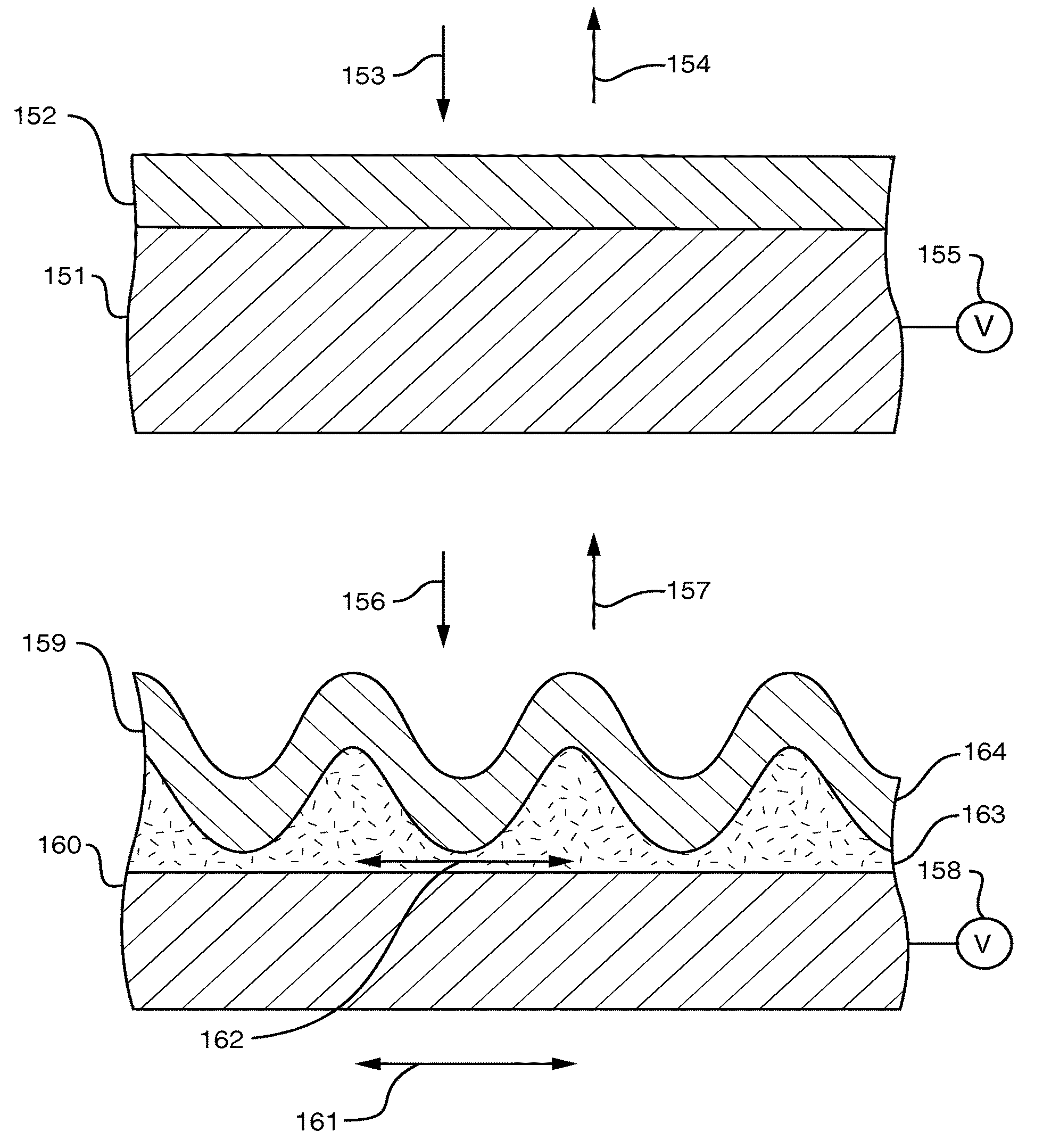
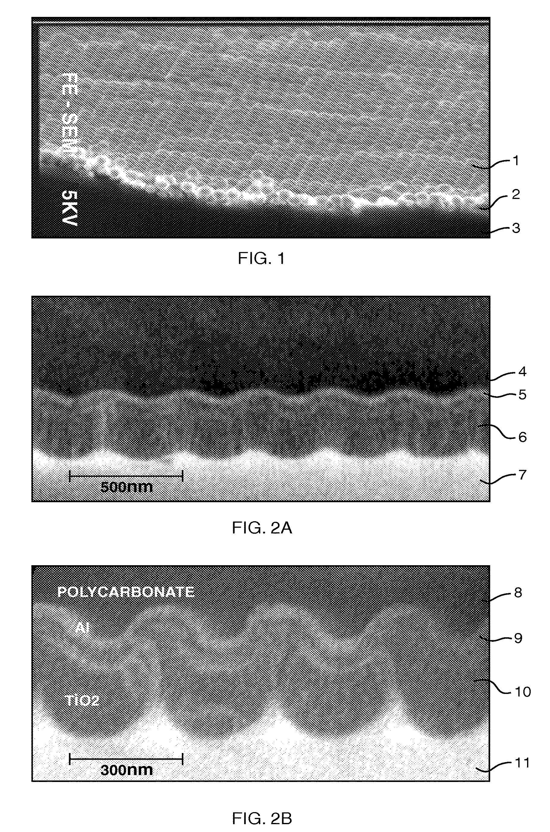
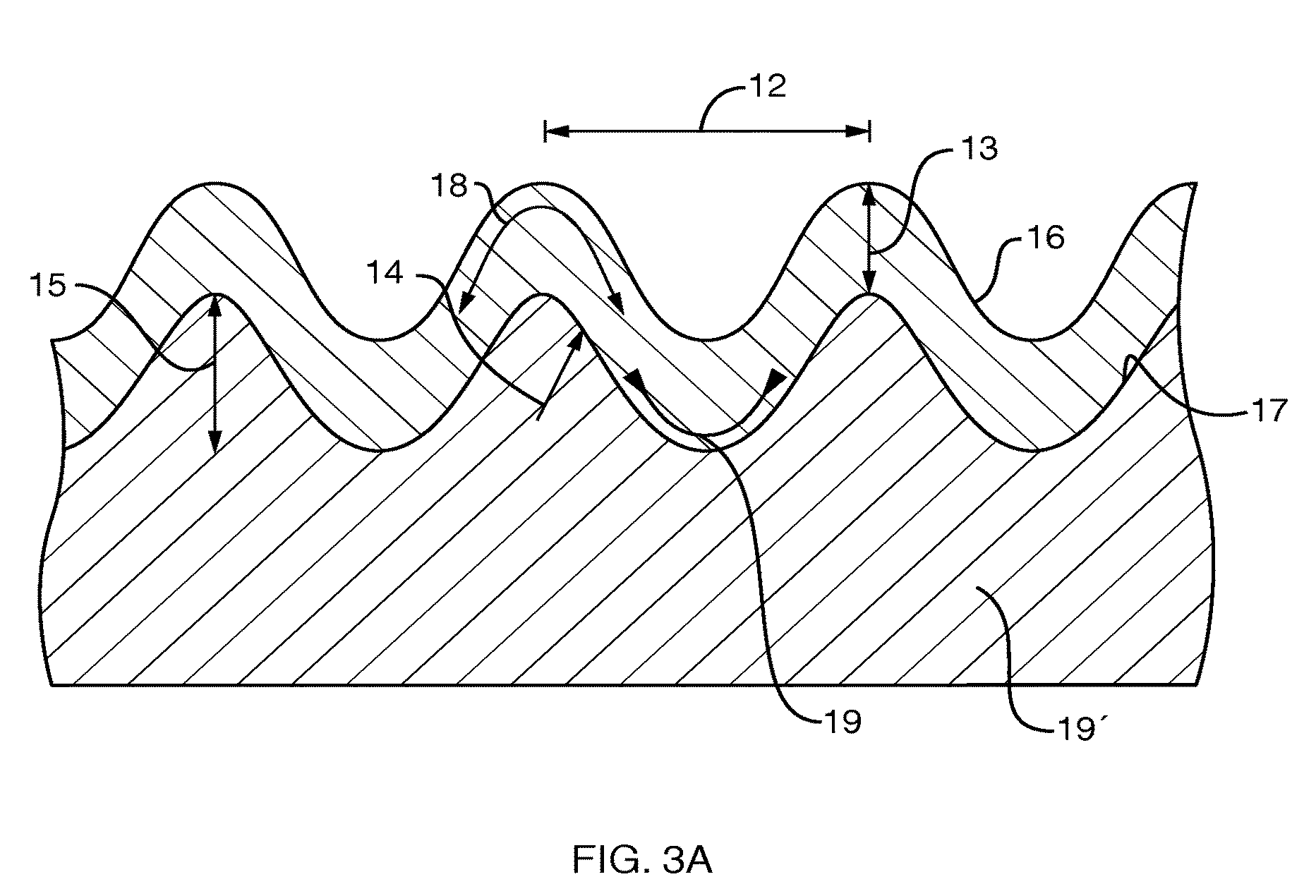
[0116]It is known that the bandgap of a semiconductor can be altered by (1) doping, (2) adding stress, and (3) adding heat. Herein, I disclose making use of the stress that is inherent in thin films, and specifically the tensile stress, to shift the bandgap of a semiconductor further into the visible spectrum. Bandgap-shift from local heating from self-focusing of the illuminant in the film is also disclosed as contributing to the effect, but this appears to be a secondary effect in this invention. For example, the energy bandgap of GaAs, or gallium arsenide, requires a 900° C. change in temperature to drop only 0.4 eV, from 1.5 eV at 100° C. down to 1.1 eV at 1000° C. On the other hand, significantly higher magnitude changes in stress can be achieved in this invention, and so stress is the predominant factor in the lowering of the bandgap energy.

[0117]When tensile stress is applied to or caused in a semiconductor, the inter-atomic spacing increases directly. An increased inter-atom...


PUM

PropertyMeasurementUnit
Pressureaaaaaaaaaa
Electrical conductivityaaaaaaaaaa
Adhesion strengthaaaaaaaaaa

Abstract

Titania is a semiconductor and photocatalyst that is also chemically inert. With its bandgap of 3.0, to activate the photocatalytic property of titania requires light of about 390 nm wavelength, which is in the ultra-violet, where sunlight is very low in intensity. A method and devices are disclosed wherein stress is induced and managed in a thin film of titania in order to shift and lower the bandgap energy into the longer wavelengths that are more abundant in sunlight. Applications of this stress-induced bandgap-shifted titania photocatalytic surface include photoelectrolysis for production of hydrogen gas from water, photovoltaics for production of electricity, and photocatalysis for detoxification and disinfection.

Description

REFERENCE TO RELATED APPLICATIONS[0001]This application is a continuation-in-part of copending application Ser. No. 10 / 424,259, filed Apr. 26, 2003 (Publication No. 2003 / 0228727), which claims benefit of Provisional Application Ser. No. 60 / 380,169, filed May 7, 2002.BACKGROUND OF INVENTION[0002]Reference is made hereinafter to the following documents:[0003]1. www.colorado.edu / bart / book / solar.htm: Bart J. Van Zeghbroeck, 1997, Chapter 4.8 (Photodiodes and Solar Cells) and Chapter Section 2.2.5 (Temperature and stress dependence of the energy bandgap).[0004]2. J. G. Mavroides, J. A. Kafalas, and D. F. Kolesar, “Photoelectrolysis of water in cells with SrTiO3 anodes,” Applied Physics Letters, Vol. 28, No. 5, 1 Mar. 1976, and references therein.[0005]3. A. Fujishima and K. Honda, Nature, 238, 37 (1972)[0006]4. O. Khaselev and J. Turner, “A Monolithic Photovoltaic-Photoelectrochemical Device for Hydrogen Production via Water Splitting,” Science, Vol. 280, 17 Apr. 1998.[0007]5. P. J. Seba...

Claims


Application Information

Patent Timeline
07 May 2009
Publication
US20090116095A1
IPC
G02F1/03; H01L31/02
CPC
G02B27/0006; H01G9/2031; H01L31/02366; Y02E10/542; H01L31/0392; H01L31/03926; G02B1/18; G02B1/11
Inventors
GUERRA, JOHN M.