Thin film type integrated energy harvest-storage device

a technology of energy harvesting and storage device and thin film, which is applied in the field of micro energy devices, can solve the problems of low energy transformation efficiency of piezoelectric materials, large size, and inability to be used in ultra small sensors or bio devices, and achieve the effect of increasing the energy transformation efficiency of piezoelectric devices

Inactive Publication Date: 2009-05-14
ELECTRONICS & TELECOMM RES INST
View PDF10 Cites 20 Cited by
  • Summary
  • Abstract
  • Description
  • Claims
  • Application Information

AI Technical Summary

Benefits of technology

[0011]The present invention provides a new type micro power device. That is, the present invention provides a new thin film type, semi-permanent, micro embedded energy generation-storage device by combining an energy generation device th

Problems solved by technology

However, such piezoelectric material currently used has a very low energy transformation efficiency and a very large size.
Therefore, the piezoelectric material can be applied to air pressure monitoring systems or functional shoes, can be very limitedly used in ultra small sensors or bio devices.
Also, since the energy generation device merely generates electric energy without having the possibility to store the generated energy, it is limitedly used in fields where a high power is instantly required or a stable power must be constantly supplied.
However, due to their very

Method used


Image

  • Thin film type integrated energy harvest-storage device
  • Thin film type integrated energy harvest-storage device
  • Thin film type integrated energy harvest-storage device

Examples


example 1

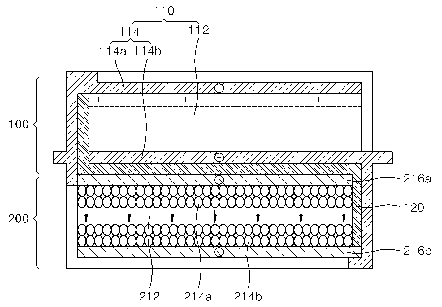
[0045]A lithium cobalt oxide (LiCoO2) layer as an anode layer is formed on an anode current collecting layer. The anode layer is formed to have a thickness of approximately 30 μm and an area of 1 cm×1 cm. A cathode layer formed of carbon having a thickness of approximately 30 μm and an area of 1 cm×1 cm is formed on a cathode collecting layer. A film type polymer electrolyte is inserted between the anode layer and the cathode layer and is packaged in a pouch, and thus, the manufacture of a thin film type battery which is an energy storage device is completed.

[0046]PMN-PT single crystal thin film, a piezoelectric material, is attached to a silicon wafer using epoxy, and the piezoelectric material is patterned to have a thickness of 10 μm with an area of 1 cm×1 cm. The patterning may be performed using a plasma etching process such as inductively coupled plasma. Next, a piezoelectric device is formed by forming interdigitated electrodes on a surface of the PMN-PT using a lift-off meth...

example 2

[0047]PMN-PT single crystal thin film is attached to a silicon substrate having an area of 2 cm×1 cm using epoxy, the PMN-PT is patterned to have a thickness of 10 μm with an area of 1 cm×1 cm. The patterning may be performed using a plasma etching process. Next, interdigitated electrodes are formed on a surface of the PMN-PT using a lift-off method. The single crystal thin film is connected to a DC conversion circuit that includes a rectifier and a condenser to complete the manufacture of an energy generation device.

[0048]The thin film battery having an area of 1 cm×1 cm manufactured as the same method as in the embodiment 1 is disposed on the silicon substrate parallel to the energy generation device which is formed on the silicon substrate. Finally, an energy generation-storage device having an area of 2 cm×1 cm with a thickness of 150 μm is configured. A final terminal can be attached to the energy storage device.

example 3

[0049]An energy generation-storage device can be manufactured by the same method as in Examples 1 and 2 using vanadium oxide having a thickness of approximately 30 μm as an anode instead of LiCoO2.


PUM


Abstract

Provided is thin film type energy generation-storage device in which an energy generation device generating energy using a piezoelectric material and an energy storage device storing the generated energy are formed in a thin film type one unit.

Description

CROSS-REFERENCE TO RELATED PATENT APPLICATION[0001]This application claims the benefit of Korean Patent Application No. 10-2007-0082932, filed on Aug. 17, 2007, in the Korean Intellectual Property Office, the disclosure of which is incorporated herein in its entirety by reference.BACKGROUND OF THE INVENTION[0002]1. Field of the Invention[0003]The present invention relates to a micro energy device, and more particularly, to a thin film type energy harvest-storage device.[0004]The present invention was supported by the Information Technology (IT) New Growing Power Core Technique Development program of the Ministry of Information and Communication (MIC). [Project No.: 2006-S-006-02, project title: Ubiquitous Terminals].[0005]2. Description of the Related Art[0006]An energy generation device (energy-harvest device) forms alternating voltages in a piezoelectric material by causing vibration, bending, contracting, extending, etc in the piezoelectric material via sound waves, ultrasonic wa...

Claims


Application Information

Patent Timeline
IPC IPC(8): H02N2/18
CPCH01M4/131H01M4/134H01M10/052Y02E60/122H01M10/46H02N2/18H01M10/0565Y02E10/50Y02E60/10H01M6/46H01L31/053
Inventor LEE, YOUNG-GIKANG, MANGULEE, SUNG Q.PARK, KANG-HOKIM, JONGDAE
Owner ELECTRONICS & TELECOMM RES INST
Why Eureka
Try Eureka