Nano-electro-mechanical memory cells and devices

a technology of electronic and mechanical components and memory cells, applied in the field of memory cells, can solve the problems of increasing process complexity and hence cost, power consumption and cost, and inability to reprogramme, and achieve the effect of low voltage levels and high density cross-poin

Inactive Publication Date: 2009-05-21
RGT UNIV OF CALIFORNIA
View PDF9 Cites 18 Cited by
  • Summary
  • Abstract
  • Description
  • Claims
  • Application Information

AI Technical Summary

Benefits of technology

[0019]A simple, scalable nano-electro-mechanical memory cell design is described which can be fabricated using conventional MOS materials and surface micromachining technology, while being particularly well-suited for use in very high density cross-point memory arr

Problems solved by technology

These characteristics pose a challenge for reducing power consumption and cost, which is particularly important for portable electronics applications.
The non-volatile memory technology illustrated in FIG. 2 is an example of a stackable technology; however, it is not re-programmable as the memory structure is based on anti-fuse storage elements in each cell.
However, a significant drawback to these technologies is their reliance on non-standard materials which increase process complexity and hence cost.
The fabrication of stackable selection devices with good performance and uniformity presents significant technological challenges.
It will be recognized that FLASH memory transistors are more difficult to scale because of the thick gate-stack equivalent oxide thickness (EOT) required in order to meet charge storage

Method used


Image

  • Nano-electro-mechanical memory cells and devices
  • Nano-electro-mechanical memory cells and devices
  • Nano-electro-mechanical memory cells and devices

Examples


Embodiment Construction

[0122]Referring more specifically to the drawings, for illustrative purposes the present invention is embodied in the apparatus generally shown in FIG. 3 through FIG. 46. It will be appreciated that the apparatus may vary as to configuration and as to details of the parts, and that the method may vary as to the specific steps and sequence, without departing from the basic concepts as disclosed herein.

1. NANO-ELECTRO-MECHANICAL MEMORY (NEMORY)

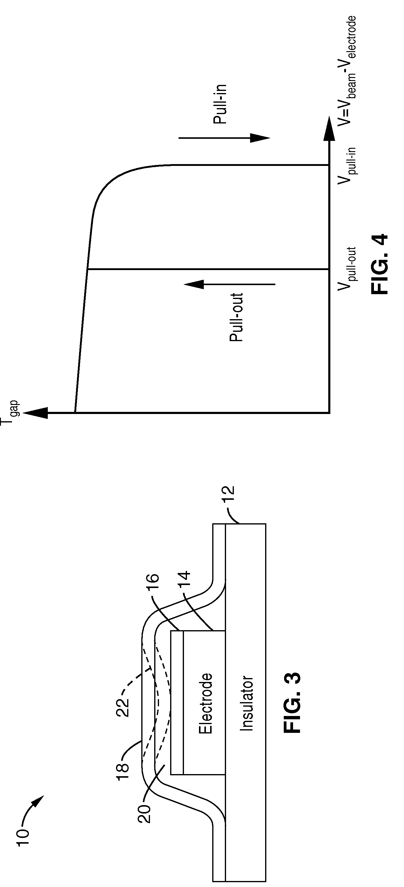
[0123]FIG. 3 through FIG. 6 illustrate aspects of a nano-electro-mechanical (NEM) nonvolatile memory cell according to the present invention, which is herein referred to for the sake of brevity as a “NEMory”. In this example a portion of the mechanical beam remains undeflected (not stuck down) when representing a data “1” state, or deflected (stuck down) in representing a data “0” state.

[0124]In FIG. 3 a first example embodiment 10 is depicted showing a substrate 12 (e.g., insulator) upon which is retained an electrode 14 with dielectric layer 1...


PUM


Abstract

A scalable nano-electro-mechanical memory cell design that requires only conventional semiconductor fabrication materials and surface micromachining technology, and is suited for use in cross-point memory arrays for very high density non-volatile storage. This design also leverages well established surface-micromachining technology and electro-mechanical device phenomena to achieve an elegantly simple and scalable memory cell structure that can potentially operate with low voltage. An elongate beam is held between a non-deflected state and a deflected state, or between two deflected states, therein defining two binary memory states. Stiction, buried charge layers, or a combination of stiction and buried charge layers can be incorporated to modify the stability of one or both deflected states for the cell. Current through the moveable portion of the elongate beam within the memory cell can be registered utilizing one or more access transistors for reading the data state.

Description

CROSS-REFERENCE TO RELATED APPLICATIONS[0001]This application claims priority from, and is a 35 U.S.C. § 111 (a) continuation of, co-pending PCT international application serial number PCT / US2007 / 067812, filed on Apr. 30, 2007, incorporated herein by reference in its entirety, which claims priority from U.S. provisional application Ser. No. 60 / 796,993 filed on May 1, 2006, incorporated herein by reference in its entirety.STATEMENT REGARDING FEDERALLY SPONSORED RESEARCH OR DEVELOPMENT[0002]Not ApplicableINCORPORATION-BY-REFERENCE OF MATERIAL SUBMITTED ON A COMPACT DISC[0003]Not ApplicableNOTICE OF MATERIAL SUBJECT TO COPYRIGHT PROTECTION[0004]A portion of the material in this patent document is subject to copyright protection under the copyright laws of the United States and of other countries. The owner of the copyright rights has no objection to the facsimile reproduction by anyone of the patent document or the patent disclosure, as it appears in the United States Patent and Tradem...

Claims


Application Information

Patent Timeline
IPC IPC(8): G11C11/00G11C7/00
CPCG11C23/00G11C2213/79G11C2213/77
Inventor KAM, HEIKING, TSU-JAE
Owner RGT UNIV OF CALIFORNIA
Why Eureka
Try Eureka