

Polishing compound and polishing method
- Summary
- Abstract
- Description
- Claims
- Application Information
AI Technical Summary
Benefits of technology
Problems solved by technology
Method used
Image

Examples
examples
[0119]Now, Examples and Comparative Examples of the present invention will be described. Further, Examples 1, 4 and 5 are Examples of the present invention, and Examples 2 and 3 are Comparative Examples.
[0120]As polishing compounds, those shown in a Table 1 were used.
TABLE 1Trishydroxy-α-HydrogenAmmoniumCitricCarbonateChlorinemethylaluminaperoxideionsacidionsionsBTAPEHAaminomethanemass %mol / kgmol / kgmol / kgmol / kgmol / kgmol / kgmol / kgmol / kgWaterpHEx. 12.770.680.850.240.0000.260.00780.00400.23Rest8Ex. 22.770.681.130.240.0000.520.00000.00000.23Rest8Ex. 32.770.680.680.240.0000.090.00780.00000.23Rest8Ex. 42.770.681.020.240.0000.260.00780.00400.00Rest8Ex. 52.770.680.700.240.0240.000.00930.00790.00Rest8All α-alumina has an average particle size of 1 μm (manufactured by Wako Pure Chemical Industries, Ltd.)BTA: BenzotriazolePEHA: Pentaethylenehexamine
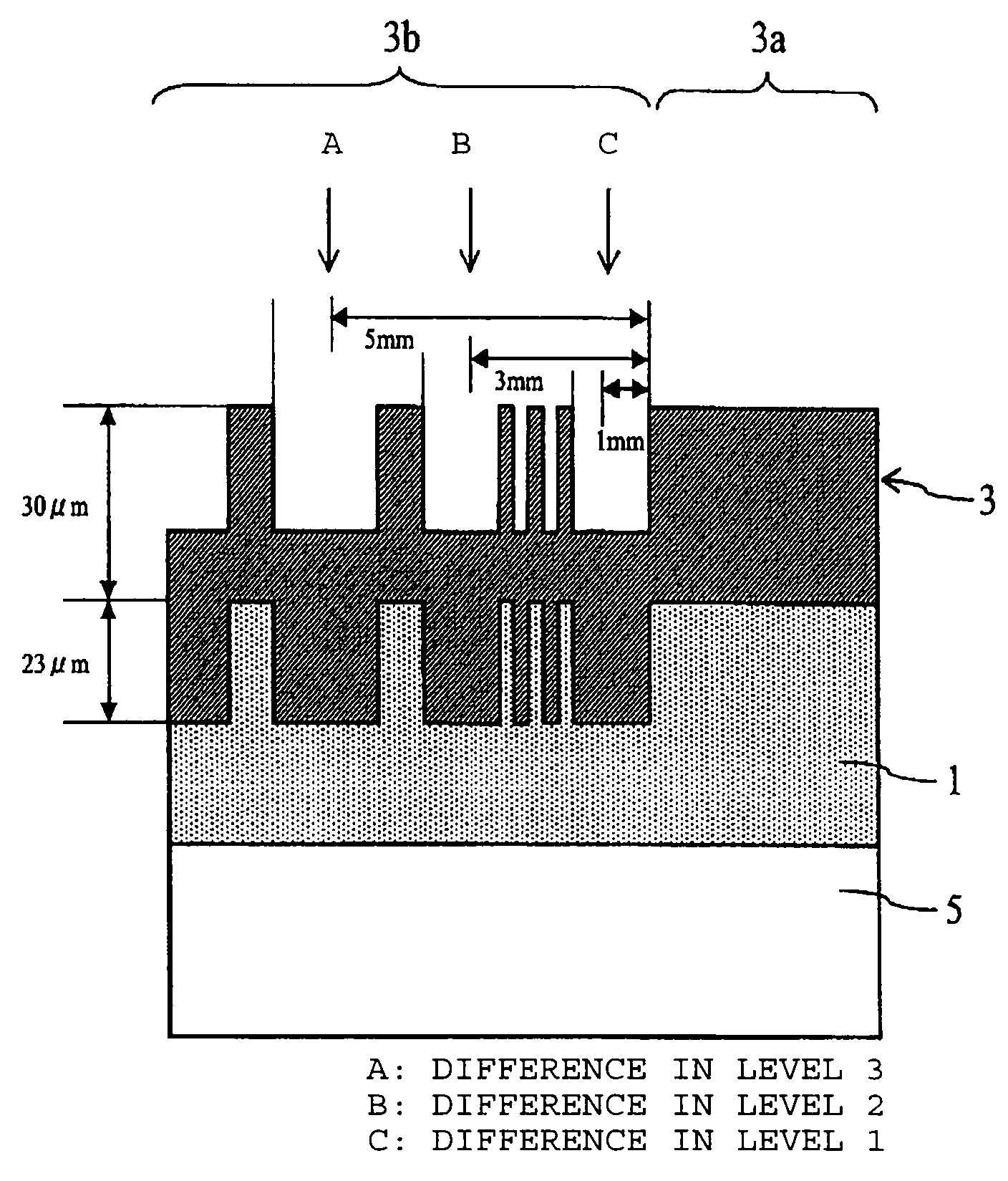
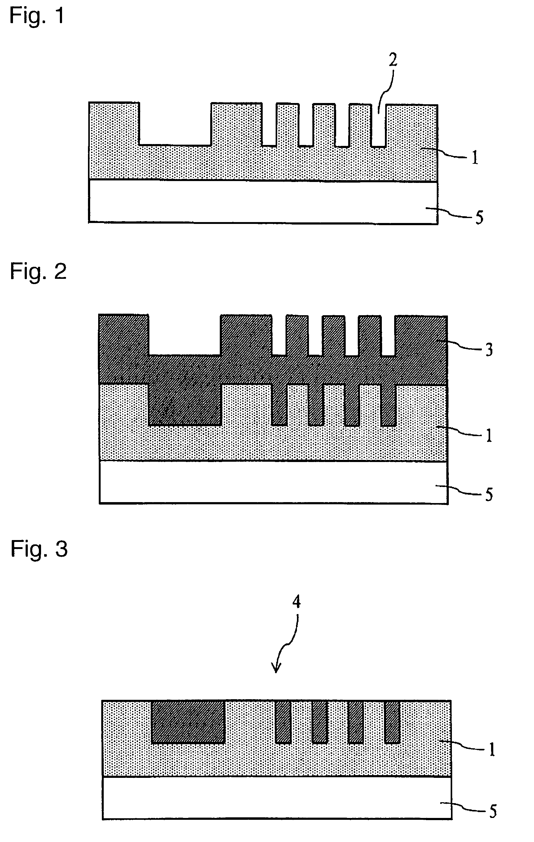
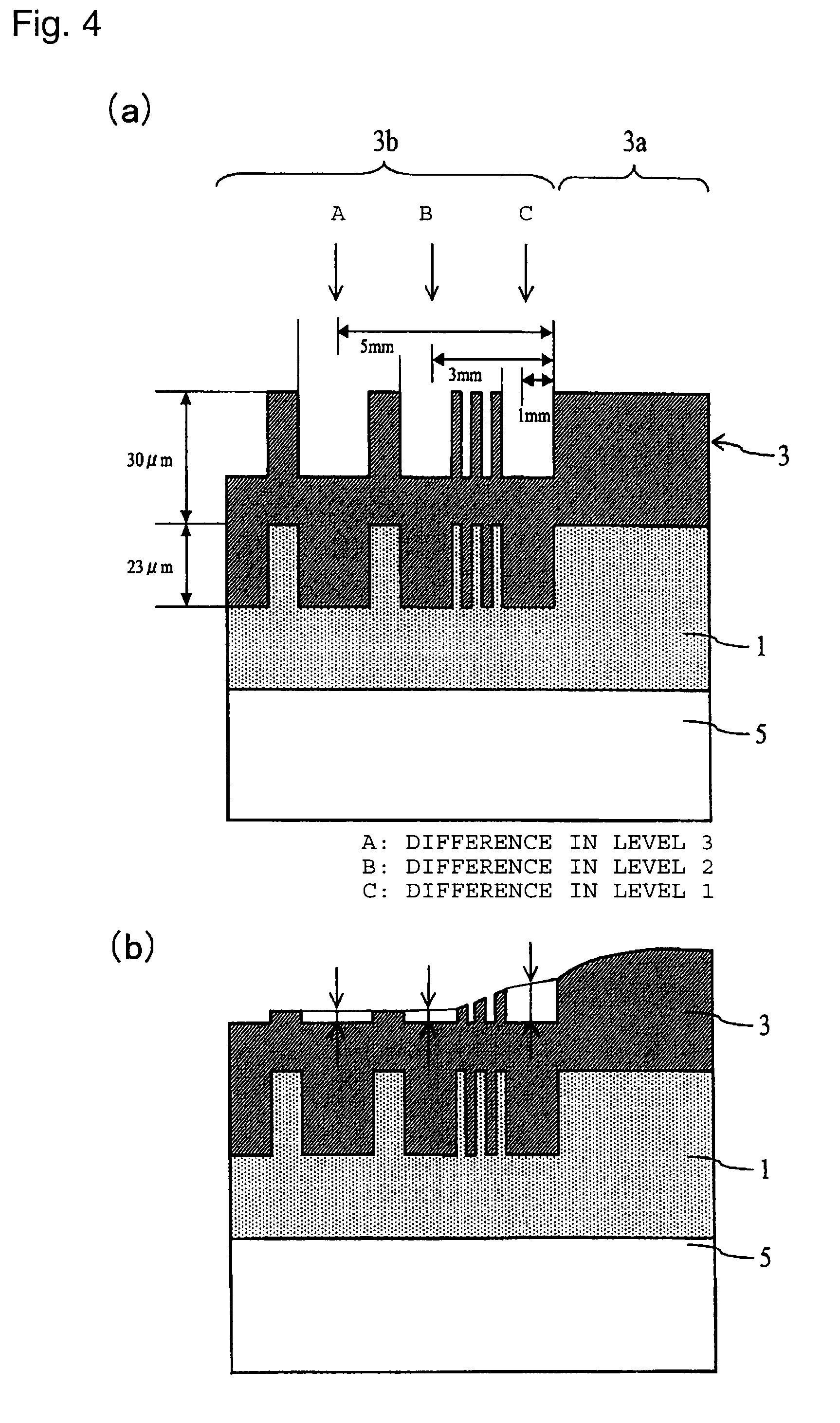
[0121]As the supporting board, a metal wafer having a thickness of 500 μm and a diameter of 6 inches was used, and on the wafer, a resin substrate h...
PUM
 Abstract
Description
Claims
Application Information