

Method of manufacturing semiconductor device
- Summary
- Abstract
- Description
- Claims
- Application Information
AI Technical Summary
Benefits of technology
Problems solved by technology
Method used
Image

Examples
first preferred embodiment
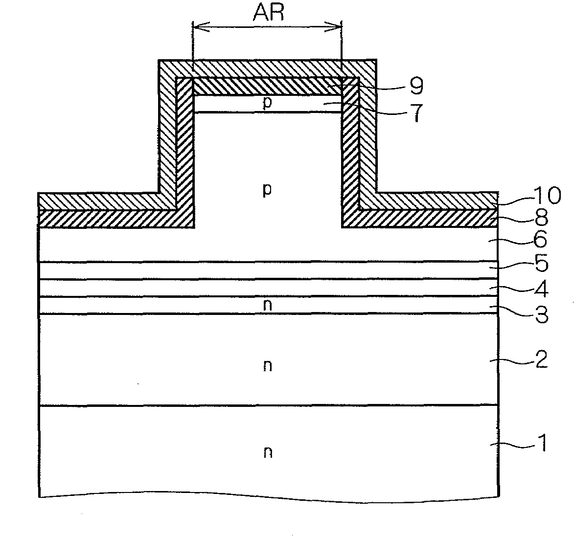
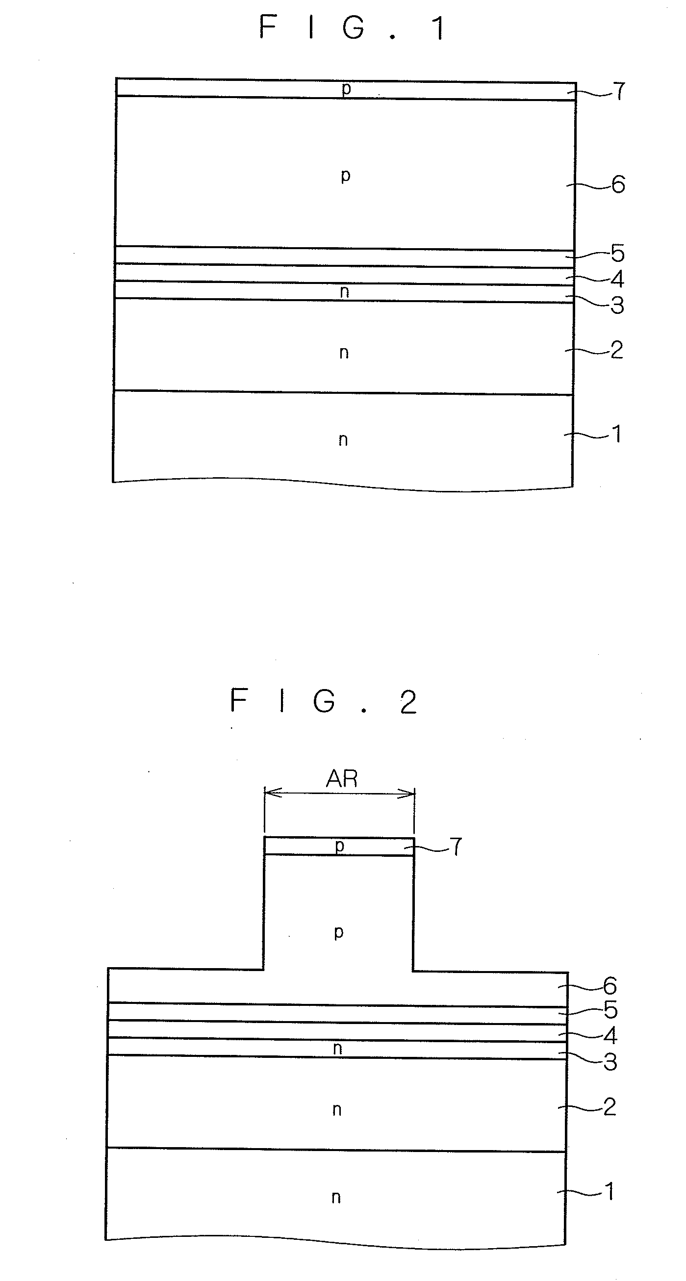
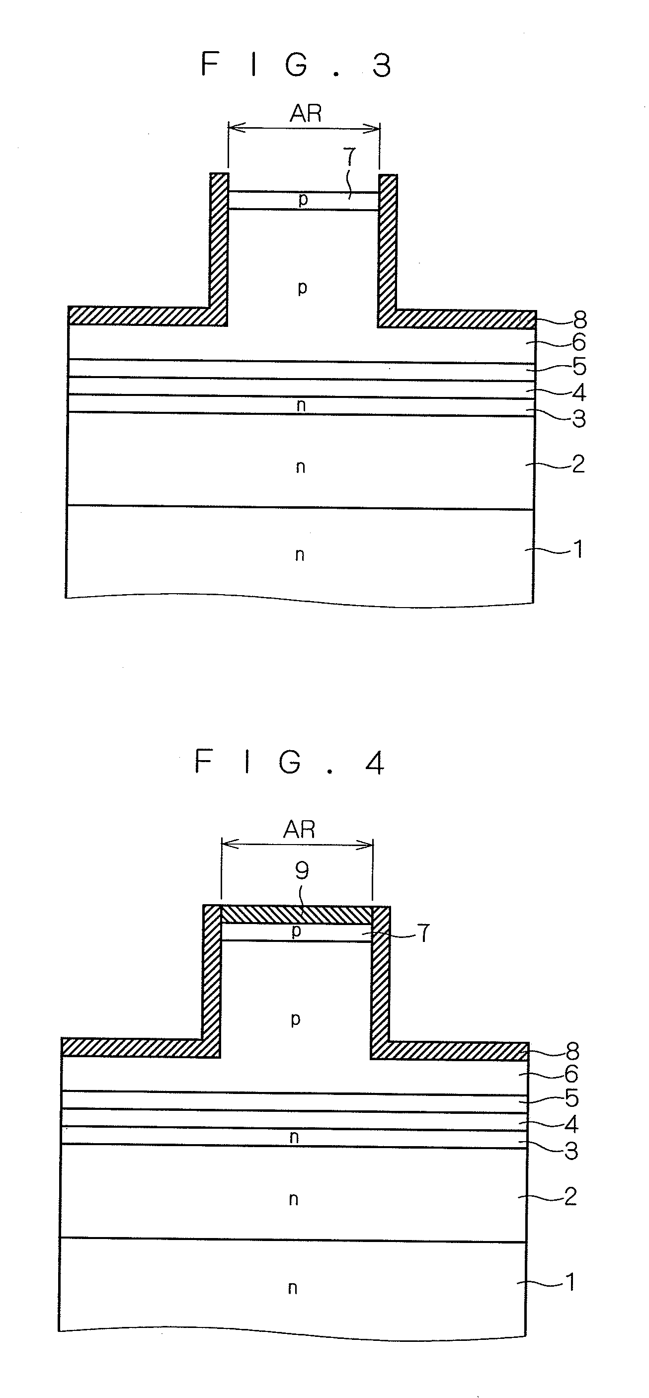
[0020]FIGS. 1 to 6 are cross-sectional views illustrating a method of manufacturing a GaN-based semiconductor device (semiconductor laser diode) according to a first preferred embodiment of the invention. Referring to these drawings, a manufacturing process in the method of manufacturing a semiconductor device according to the first preferred embodiment is described below.
[0021]First, as shown in FIG. 1, a layered structure (semiconductor structure) including an n-type AlGaN cladding layer 2, an n-type GaN guide layer 3, an InGaN quantum-well active layer 4, a GaN guide layer 5, a p-type AlGaN cladding layer 6, and a p-type GaN contact layer 7 is formed on an n-type low-resistance GaN substrate 1.
[0022]The n-type AlGaN cladding layer 2 is a layer for carrier and optical confinement, and the n-type GaN guide layer 3 is a layer for light propagation. The n-type GaN guide layer 3 may be replaced with an n-type InGaN guide layer.
[0023]The InGaN quantum-well active layer 4 is a light-emi...
second preferred embodiment
[0041]FIG. 7 is a cross-sectional view illustrating part of a method of manufacturing a GaN-based semiconductor device (semiconductor laser diode) according to a second preferred embodiment of the invention. Referring now to FIG. 7, a manufacturing process in the method of manufacturing a semiconductor device according to the second preferred embodiment is described.
[0042]After the steps of the first preferred embodiment in FIGS. 1 to 3, then as shown in FIG. 7, a metallic compound 19, which is also an oxide, is formed on the surface of the p-type GaN contact layer 7 by a deposition of a metallic compound that contains oxygen or both oxygen and nitrogen, such as GaO, RuO, PdO, GaON, RuON, or PdON.
[0043]Then, through the steps of the first preferred embodiment in FIGS. 5 and 6, the same processing as described in the first preferred embodiment is performed, completing the manufacture of a GaN-based semiconductor device according to the second preferred embodiment. It is noted herein ...
third preferred embodiment
[0050]FIG. 8 is a cross-sectional view illustrating part of a method of manufacturing a GaN-based semiconductor device according to a third preferred embodiment of the invention. Referring now to FIG. 8, a manufacturing process in the method of manufacturing a semiconductor device according to the third preferred embodiment is described.
[0051]After the steps of the first preferred embodiment in FIGS. 1 to 3, then as shown in FIG. 8, an oxide film 21 is formed on the surface of the p-type GaN contact layer 7 by oxidation of the surface of the p-type GaN contact layer 7 with the supply of an oxygen-containing gas such as O2, O3, NO, N2O, or NO2.
[0052]Further, a metallic compound 22 is formed on the oxide film 21 by a deposition of a metallic compound that contains oxygen or both oxygen and nitrogen such as GaO, RuO, PdO, GaON, RuON, or PdON. These oxide film 21 and the metallic compound 22 form a layered oxide structure 20.
[0053]After that, through the steps of the first preferred emb...
PUM
 Abstract
Description
Claims
Application Information