Light emitting diode structure and method for fabricating the same

a technology of light-emitting diodes and diodes, which is applied in the direction of semiconductor/solid-state device manufacturing, semiconductor devices, electrical devices, etc., can solve the problems of insufficient light efficiency, complicated process, and inability to meet the requirements of the market, so as to reduce the total reflection, reduce the horizontal light propagation between the substrate and the semiconductor layer, and increase the light extraction efficiency of the led element

Inactive Publication Date: 2009-06-25
TEKCORE CO LTD
View PDF3 Cites 32 Cited by
  • Summary
  • Abstract
  • Description
  • Claims
  • Application Information

AI Technical Summary

Benefits of technology

[0019]The advantage of the present invention is to use a novel process to form a chemical reaction layer on the surface of the substrate, and use the chemical reaction layer as a natural etching mask to form an irregular geometry of serrations on the surface of the substrate via a dry- or wet-etching method. The light generated by the LED element will be scattered or diffracted by the irregular serrations. Thus, the horizontal light propagation between the substrate and the semiconductor layers is decreased, and the total reflection is reduced, and the light extraction efficiency of the LED element is increased. Besides, growing epitaxial materials on the serrated surface of the substrate can reduce threading dislocations, promote the quality of the epitaxial material, and increase the internal quantum efficiency. Further, the present invention has a simple process and thus can reduce fabrication cost and benefit mass-production.
is to use a novel process to form a chemical reaction layer on the surface of the substrate, and use the chemical reaction layer as a natural etching mask to form an irregular geometry of serrations on the surface of the substrate via a dry- or wet-etching method. The light generated by the LED element will be scattered or diffracted by the irregular serrations. Thus, the horizontal light propagation between the substrate and the semiconductor layers is decreased, and the total reflection is reduced, and the light extraction efficiency of the LED element is increased. Besides, growing epitaxial materials on the serrated surface of the substrate can reduce threading dislocations, promote the quality of the epitaxial material, and increase the internal quantum efficiency. Further, the present invention has a simple process and thus can reduce fabrication cost and benefit mass-production.

Problems solved by technology

Thus, LED has an insufficient light efficiency.
However, such a process is more complicated and cost-inefficient, which will impair the commercialization of LED.

Method used


Image

  • Light emitting diode structure and method for fabricating the same
  • Light emitting diode structure and method for fabricating the same
  • Light emitting diode structure and method for fabricating the same

Examples


embodiment i

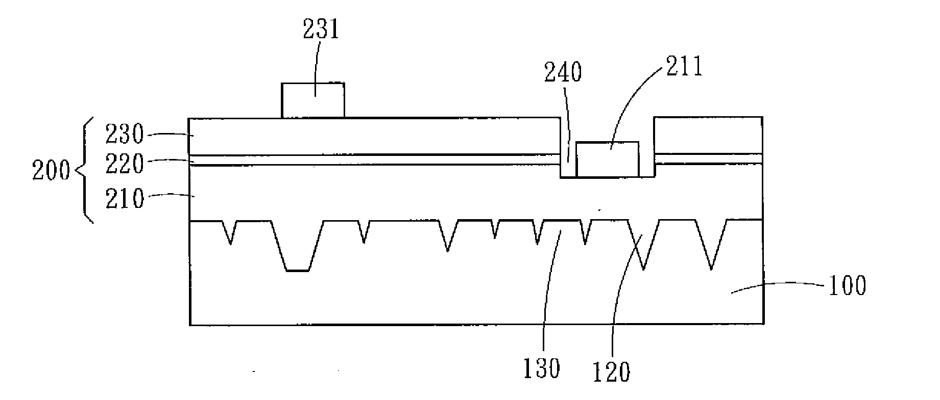
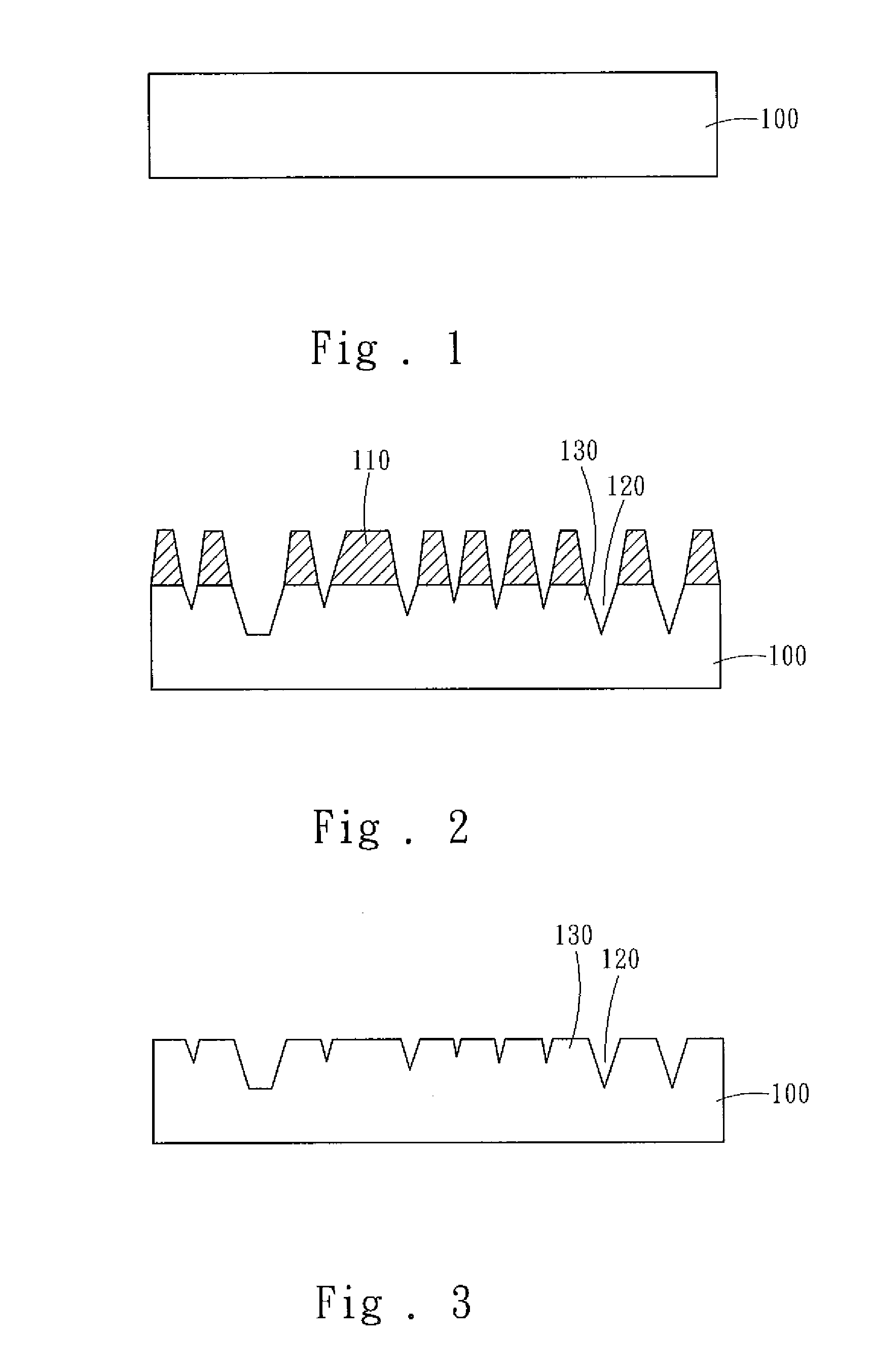
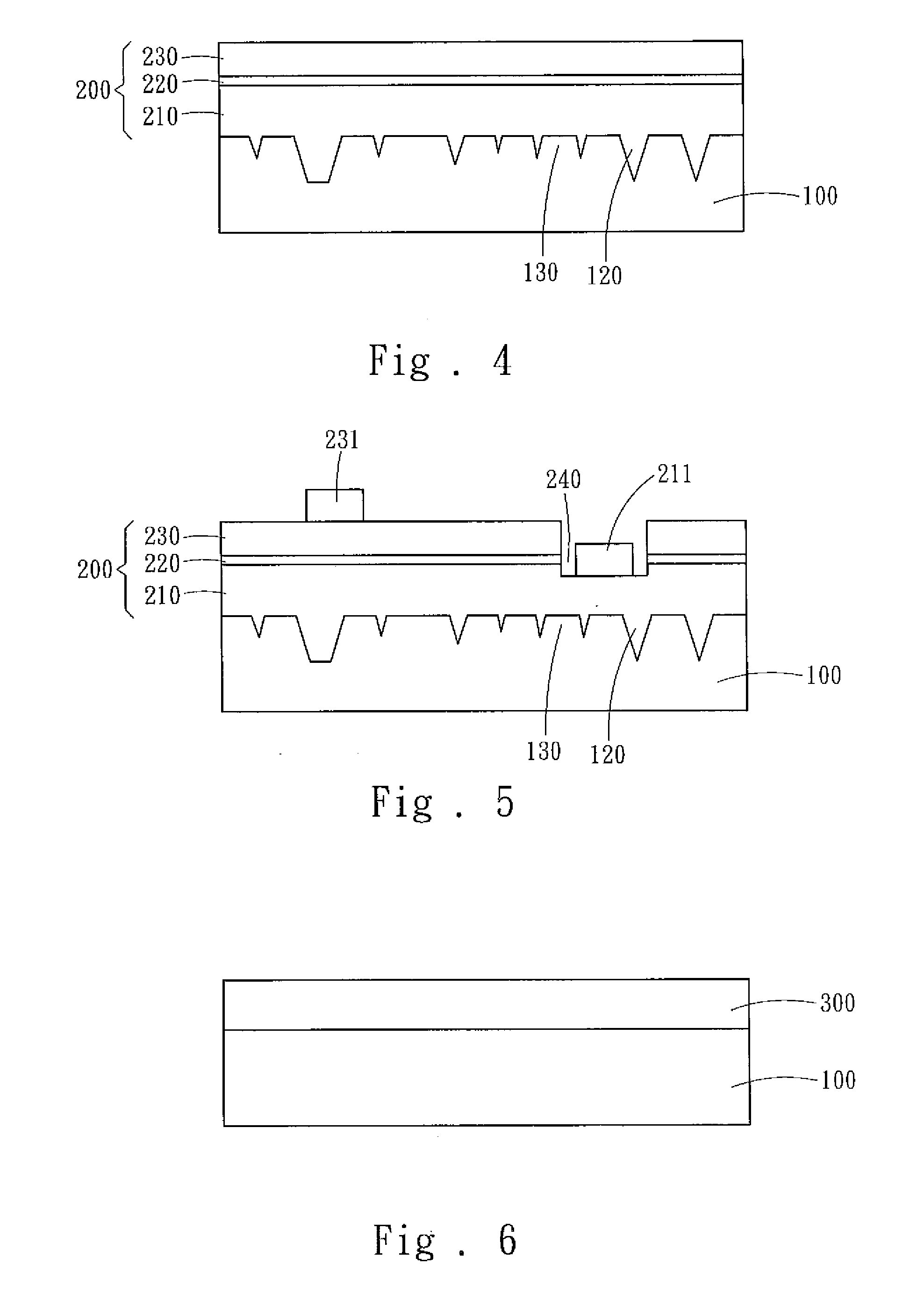
[0027]Refer to from FIG. 1 to FIG. 5 diagrams schematically showing a first embodiment of the present invention. The method of the present invention includes providing a substrate 100, as shown in FIG. 1. The substrate 100 may be made of sapphire, silicon carbide, silicon, gallium arsenide, aluminum nitride, or gallium nitride.

[0028]Next, the substrate 100 is placed in a first solution for chemical reaction, and a high-density nanometric chemical reaction layer 110 naturally forms on the surface of the substrate 100. The substrate 100 should be placed in the first solution for from 1 second to 200 minutes. Next, the substrate 100 is selectively etched to form a plurality of concave zones 120 on the substrate 100 without the chemical reaction layer 110 and form a plurality of convex zones 130 having the chemical reaction layer 110 overhead with the chemical reaction layer 110 being a mask and with a dry-etching method, a wet-etching method, or a combination of a dry-etching method an...

embodiment ii

[0036]Refer to from FIG. 6 to FIG. 8 diagrams schematically showing a second embodiment of the present invention. The method of the second embodiment is based on that of the first embodiment, but a pre-treatment is first performed before the substrate 100 is placed in the first solution. The pre-treatment is to grow a passivation layer 300 having a thickness of between 1 Å and 10 μm on the surface of the substrate 100, as shown in FIG. 6. The passivation layer 300 may be a single- or multi-layer structure made of one or more materials selected from the group including: silicon, silicon nitride, silicon oxide, aluminum oxide, metal, photoresist, benzocyclobutene, and polyimide.

[0037]Then, the substrate 100 is placed in the first solution to form a high-density nanometric chemical reaction layer 110 inside the passivation layer 300 on the surface of the substrate 100. Next, the substrate 100 is selectively etched with the passivation layer 300 and the chemical reaction layer 110 being...

embodiment iii

[0039]Refer to from FIG. 9 to FIG. 13 diagrams schematically showing a third embodiment of the present invention. The method of the third embodiment is based on that of the second embodiment, and the pretreatment is also to grow a passivation layer 300 on the surface of the substrate 100, as shown in FIG. 9. Next, the passivation layer 300 is patterned with a photolithographic process to form periodical patterns to expose parts of the surface of the substrate 100, as shown in FIG. 10. The periodical patterns of the passivation layer 300 may be the periodical pattern of circles, polygons, or the combination of them. The width of the periodical pattern is within from 0.1 to 15 μm, and the spacing between the periodical patterns is also within from 0.1 to 15 μm.

[0040]Next, the substrate 100 is placed in the first solution to form a high-density nanometric chemical reaction layer 110 on the exposed surfaces of the substrate 100, as shown in FIG. 11. Next, the substrate 100 is selectivel...


PUM


Abstract

The present invention discloses a light emitting diode structure and a method for fabricating the same. In the present invention, a substrate is placed in a solution to form a chemical reaction layer. Next, the substrate is etched to form a plurality of concave zones and a plurality of convex zones with the chemical reaction layer overhead. Next, the chemical reaction layer is removed to form an irregular geometry of the concave zones and convex zones on the surface of the substrate. Then, a semiconductor light emitting structure is epitaxially formed on the surface of the substrate. Thereby, the present invention can achieve a light emitting diode structure having improved internal and external quantum efficiencies.

Description

FIELD OF THE INVENTION[0001]The present invention relates to a light emitting diode structure, particularly to a light emitting diode structure and a method for fabricating the same, wherein a natural etching mask is used in a selective etching to form on the surface of the substrate an irregular geometry of concave zones and convex zones, which can change the light propagation direction inside the semiconductor layer and increase the external quantum efficiency of the light emitting diode.BACKGROUND OF THE INVENTION[0002]Improving LED (Light Emitting Diode) light efficiency is a top priority for realizing a solid-state illuminator. There are two approaches to improve LED light efficiency: one is to increase LED internal quantum efficiency, and the other is to increase LED external quantum efficiency (LED light extraction efficiency).[0003]Improving the quality of epitaxial material can most directly and obviously promote internal quantum efficiency. An ELOG (Epitaxial Lateral Over-...

Claims


Application Information

Patent Timeline
Patent Type & Authority Applications(United States)
IPC IPC(8): H01L33/00H01L33/12H01L33/22
CPCH01L21/0237H01L21/0242H01L33/22H01L21/02658H01L33/12H01L21/02647
Inventor LEE, CHIA-MINGLIN, HUNG-CHENGCHYI, JEN-INN
Owner TEKCORE CO LTD
Why Eureka
Try Eureka