Electroluminescent display compensated analog transistor drive signal

a technology of analog transistors and drive signals, applied in the direction of instruments, static indicating devices, etc., can solve the problems of increasing the electronics size of subpixels, increasing the complexity of subpixels, and oled efficiency loss, so as to reduce the aperture ratio of subpixels, simplify the compensation of control signals, and reduce the effect of oled efficiency loss

Active Publication Date: 2009-06-25
GLOBAL OLED TECH
View PDF14 Cites 52 Cited by
  • Summary
  • Abstract
  • Description
  • Claims
  • Application Information

AI Technical Summary

Benefits of technology

[0030]The present invention provides an effective way of providing the analog drive transistor control signal. It requires only one measurement to perform compensation. It can be applied to any active-matrix backplane. The compensation of the control signal has been simplified by using a look-up table (LUT) to change signals from nonlinear to linear so compensation can be in linear voltage domain. It compensates for Vth shift, Voled shift, and OLED efficiency loss without requiring complex pixel circuitry or external measurement devices. It does not decrease the aperture ratio of a subpixel. It has no effect on the normal operation of the panel.

Problems solved by technology

Methods such as this compensate for Vth shift, but they cannot compensate for Voled rise or OLED efficiency loss.
These methods require increased subpixel complexity and increased subpixel electronics size compared to the conventional 2T1C voltage-drive subpixel circuit.
Increased subpixel complexity reduces yield, because the finer features required are more vulnerable to fabrication errors.
Particularly in typical bottom-emitting configurations, increased total size of the subpixel electronics increases power consumption because it reduces the aperture ratio, the percentage of each subpixel which emits light.
Additionally, higher currents in smaller areas increase current density in the OLED device, which accelerates Voled rise and OLED efficiency loss.
These methods share the disadvantages of in-pixel Vth compensation schemes, but some can additionally compensate for Voled shift or OLED efficiency loss.
These methods cannot compensate for Voled rise or OLED efficiency loss.
Reverse-bias methods can compensate for the average Vth shift of the panel with less increase in power consumption than in-pixel compensation methods, but they require more complicated external power supplies, can require additional pixel circuitry or signal lines, and may not compensate individual subpixels that are more heavily faded than others.
However, when the drive transistors in the circuit are formed from a-Si, this assumption is not valid, as the threshold voltage of the transistors also changes with use.
The method of Arnold will thus not provide complete compensation for subpixel aging in circuits wherein transistors show aging effects.
Additionally, when methods such as reverse bias are used to mitigate a-Si transistor threshold voltage shifts, compensation of OLED efficiency loss can become unreliable without appropriate tracking / prediction of reverse bias effects, or a direct measurement of the OLED voltage change or transistor threshold voltage change.
An external light sensor adds to the cost and complexity of a device, while integrated light sensors increase subpixel complexity and electronics size, with attendant performance reductions.
Existing Vth compensation schemes are not without drawbacks, and few of them compensate for Voled rise or OLED efficiency loss.
Those that compensate each subpixel for Vth shift do so at the cost of panel complexity and lower yield.

Method used


Image

  • Electroluminescent display compensated analog transistor drive signal
  • Electroluminescent display compensated analog transistor drive signal
  • Electroluminescent display compensated analog transistor drive signal

Examples


Embodiment Construction

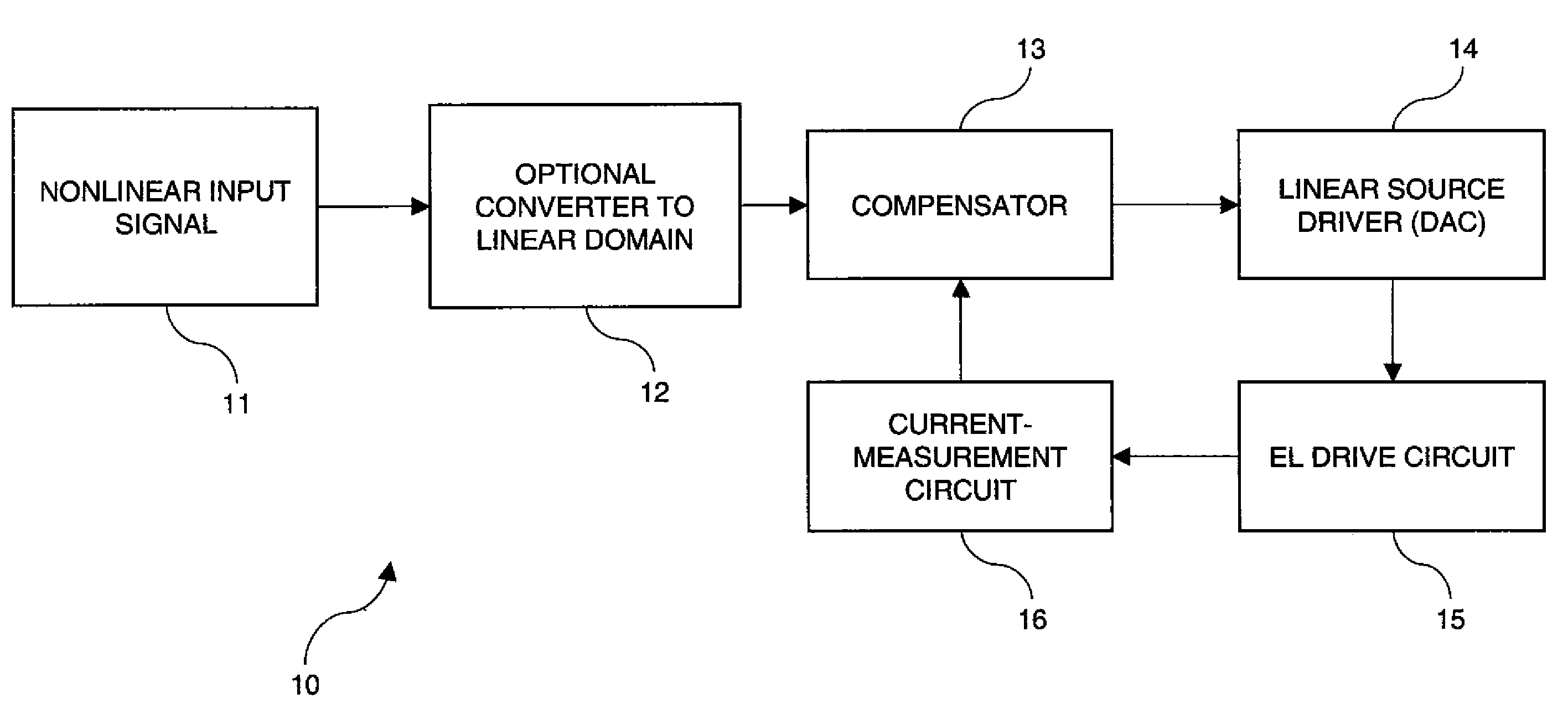
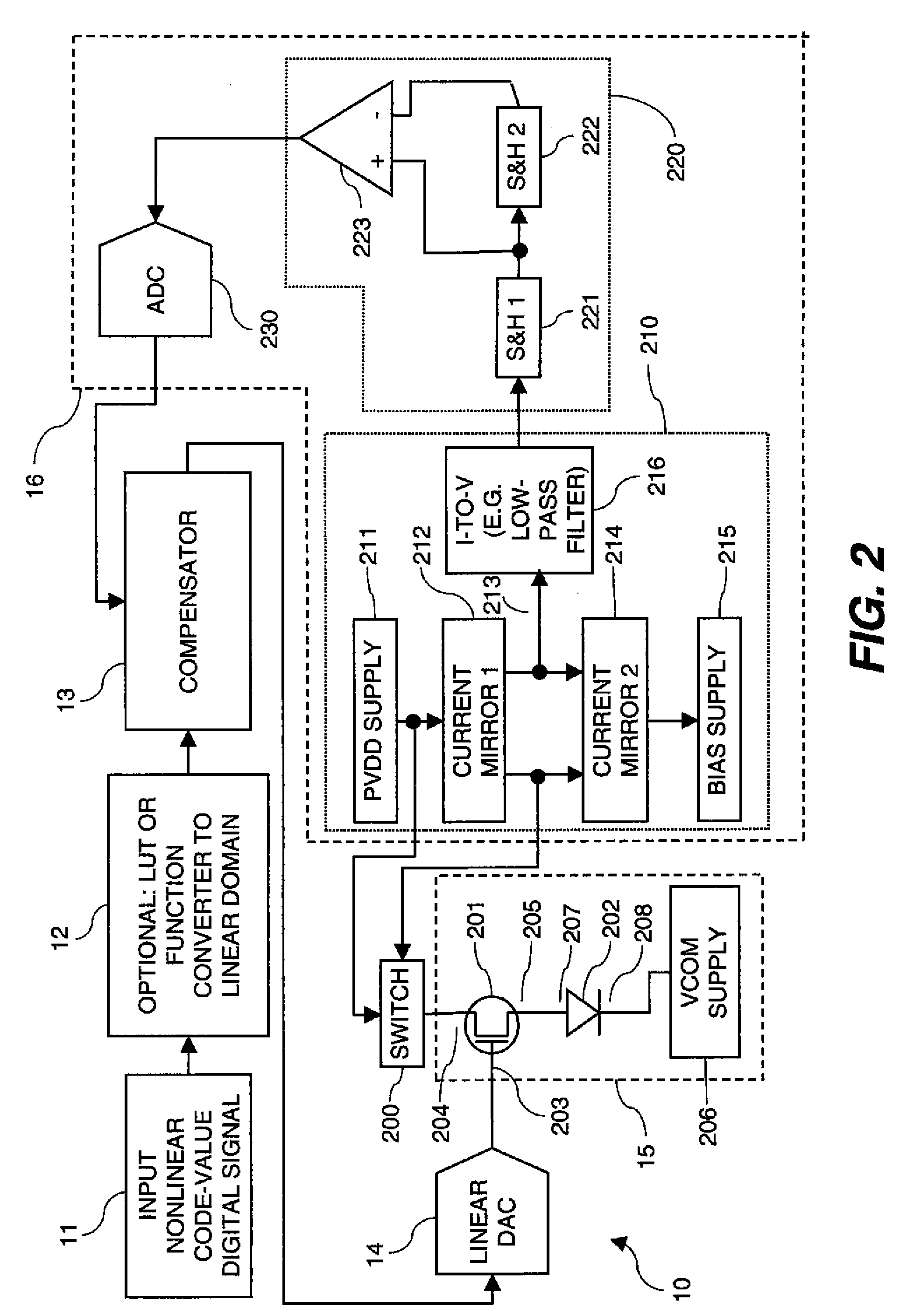
[0046]The present invention compensates for degradation in the drive transistors and EL devices on an active-matrix EL display panel. In one embodiment, it compensates for Vth shift, Voled shift, and OLED efficiency loss of all subixels on an active-matrix OLED panel. A panel comprises a plurality of pixels, each of which comprises one or more subpixels. For example, each pixel might comprise a red, a green, and a blue subpixel. Each subpixel comprises an EL device, which emits light, and surrounding electronics. A subpixel is the smallest addressable element of a panel. The EL device can be an OLED device.

[0047]The discussion to follow first considers the system as a whole. It then proceeds to the electrical details of a subpixel, followed by the electrical details for measuring one subpixel and the timing for measuring multiple subpixels. It next covers how the compensator uses measurements. Finally, it describes how this system is implemented in one embodiment, e.g. in a consumer...


PUM


Abstract

Apparatus for providing an analog drive transistor control signal to the gate electrode of a drive transistor in a drive circuit that applies current to an EL device, the drive circuit including a first supply electrode of the drive transistor and the EL device connected to a second supply electrode of the drive transistor, comprising a measuring circuit for measuring the current passing through the supply electrodes at different times to provide an aging signal representing variations in the characteristics of the drive transistor and EL device caused by operation of the drive transistor and EL device over time; a compensator for changing a linear code value in response to the aging signal to compensate for the variations in the characteristics of the drive transistor and EL device; and a linear source driver for producing the analog drive transistor control signal in response to the changed linear code value.

Description

CROSS REFERENCE TO RELATED APPLICATIONS[0001]Reference is made to commonly-assigned, co-pending U.S. patent application Ser. No. 11 / 626,563 entitled “OLED Display with Aging and Efficiency Compensation” to Leon et al, dated Jan. 24, 2007, incorporated by reference herein.FIELD OF THE INVENTION[0002]The present invention relates to control of an analog signal applied to a drive transistor for supplying current through an electroluminescent device.BACKGROUND OF THE INVENTION[0003]Flat-panel displays are of great interest as information displays for computing, entertainment, and communications. Electroluminescent (EL) flat-panel display technologies, such as organic light-emitting diode (OLED) technology provides benefits in color gamut, luminance, and power consumption over other technologies such as liquid-crystal display (LCD) and plasma display panel (PDP). However, EL displays suffer from performance degradation over time. In order to provide a high-quality image over the life of ...

Claims


Application Information

Patent Timeline
Patent Type & Authority Applications(United States)
IPC IPC(8): G09G3/30
CPCG09G3/3233G09G3/3291G09G2320/045G09G2320/029G09G2320/043G09G2300/0417
Inventor LEON, FELIPE A.WHITE, CHRISTOPHER J.PARRETT, GARYPRIMERANO, BRUNO
Owner GLOBAL OLED TECH
Why Eureka
Try Eureka