


Quick Research
Generate reliable direction feasibility study reports for your R&D in just a few steps.

Technical Q&A
Discover and master advanced knowledge NOW. Basics, ideas, possibilities, all at once.

Find Solutions
As an expert in R&D theories, this can generate solutions to your technical problems instantly.

Evaluate Feasibility
Analyze your overall solution with one click, know your potential R&D risks in advance.

Monitor Landscape
Get weekly tech updates, stay abreast of the latest tech innovations and key insights.
Package substrate embedded with semiconductor component
- Summary
- Abstract
- Description
- Claims
- Application Information
AI Technical Summary
Benefits of technology
Problems solved by technology
Method used
Image

Examples
first embodiment
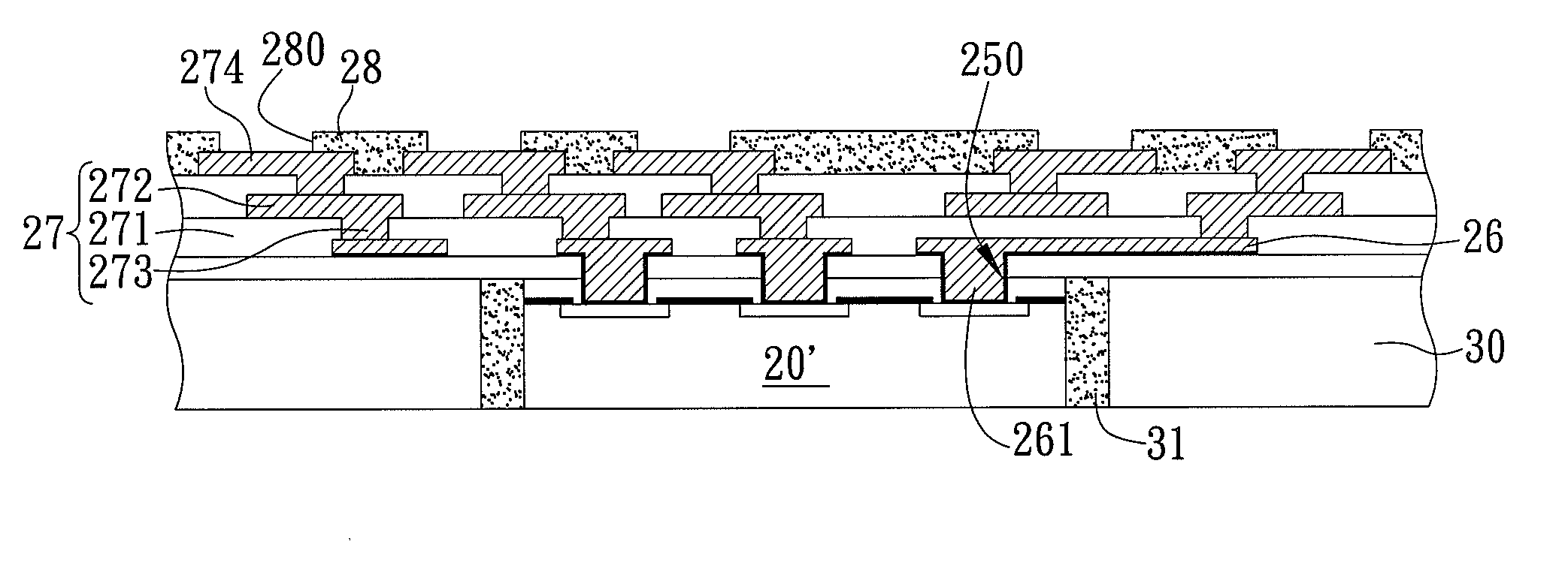
[0023]Referring to FIGS. 2A to 2C and 3A to 3H, a package substrate embedded with a semiconductor component according to a first embodiment of the present invention are shown.
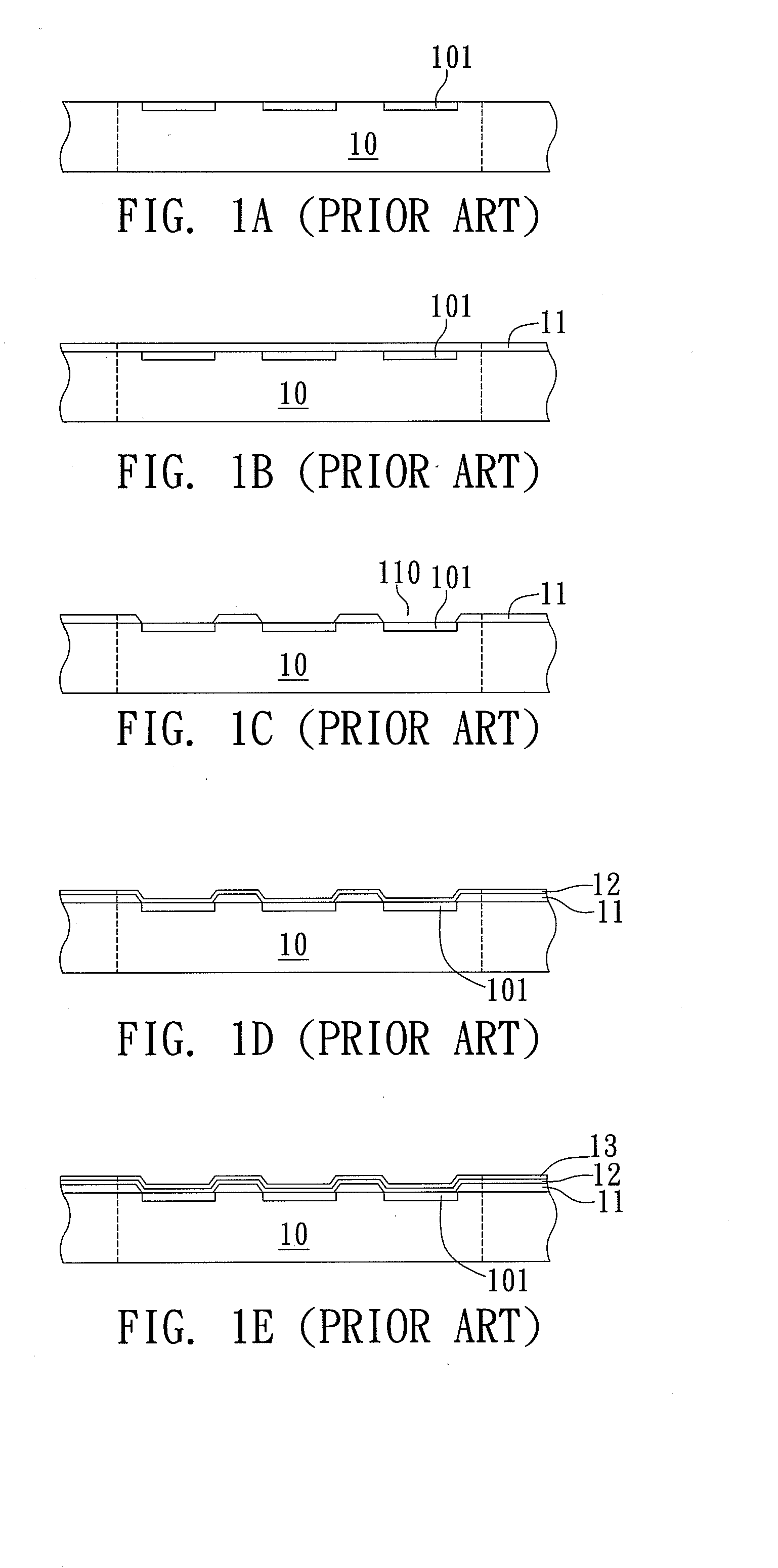
[0024]Referring to FIGS. 2A to 2C, a passivation layer on a wafer is shown.
[0025]As shown in FIG. 2A, a wafer 20 having an active face 20a and an inactive face 20b opposite to each other is provided. A plurality of electrode pads 201 are formed on the active face 20a.
[0026]As shown in FIG. 2B, a first passivation layer 22a, such as silicon nitride (Si3N4), is formed on the active face 20a of the wafer 20 having a plurality of openings 220a to expose partial surfaces of the electrode pads 202.
[0027]As shown in FIG. 2C, a second passivation layer 22b, such as polyimide, is formed on the electrode pads 201 and the first passivation layer 22a. The first and second passivation layers 22a and 22b constitute a passivation layer 22.
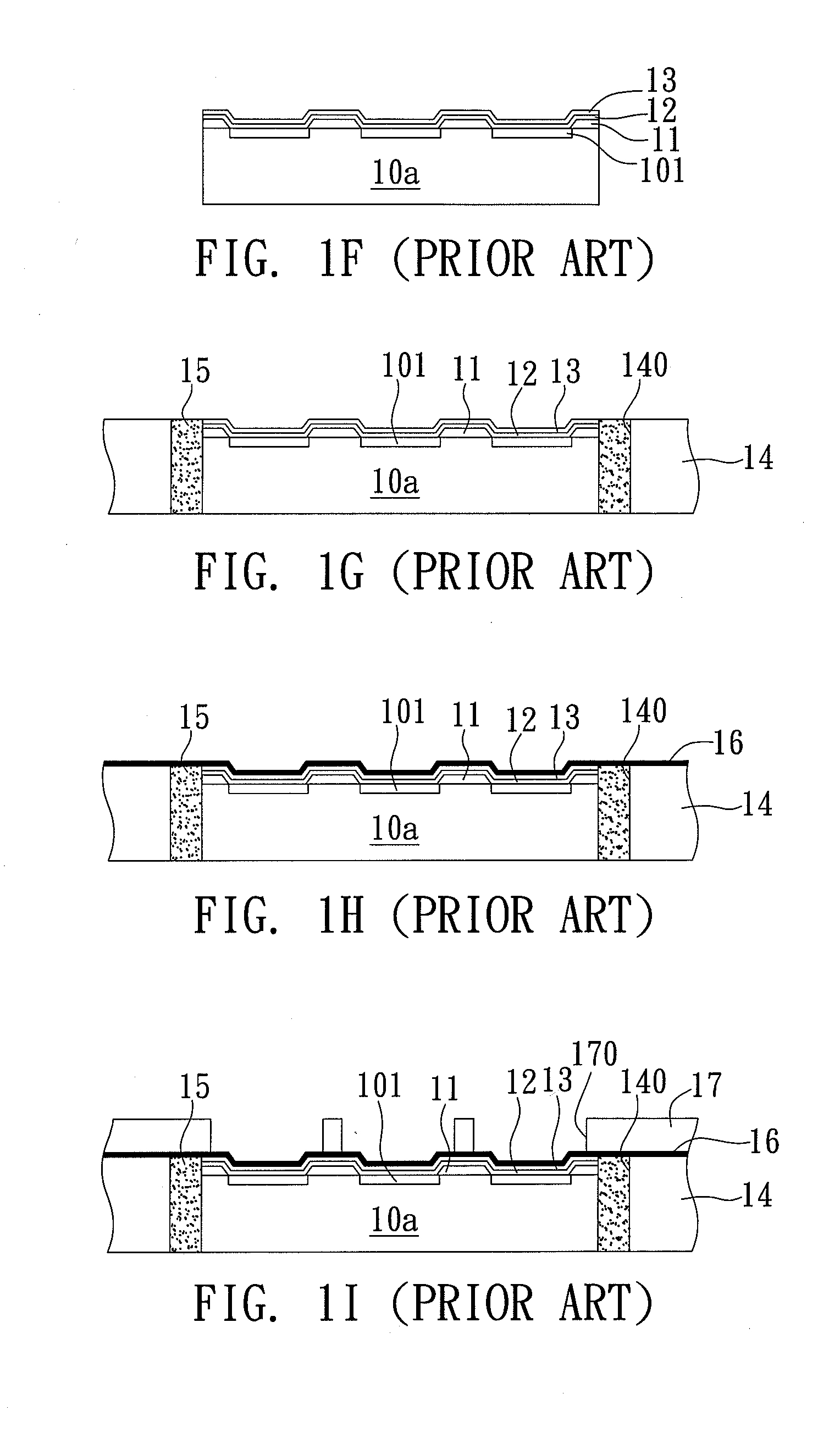
[0028]Referring to FIGS. 3A to 3H, cross-sectional views illustrating a semiconductor c...
second embodiment
[0038]Referring to FIGS. 4A to 4G, cross-sectional views of a package substrate embedded with a semiconductor component according to a second embodiment of the present invention are shown. The second embodiment is similar to the first embodiment, but the main difference lies in the dielectric layer and its openings on the substrate and the semiconductor chip.
[0039]As shown in FIG. 4A, a structure shown in FIGS. 3B, 3B′ or 3B″ is provided. The structure shown in FIG. 3B is used for illustration purpose.
[0040]As shown in FIG. 4B, a first dielectric layer 23′ made of a photosensitive material is formed on top of the substrate 30 and the passivation layer 22 by printing, spin coating or adhesion. Penetrating openings 230′ are formed at locations corresponding to those of the electrode pads 201 by lithography techniques such as exposure and development.
[0041]As shown in FIG. 4C, openings 220 are then formed in the passivation layer 22 within the openings 230′ to expose the electrode pads...
PUM
 Abstract
Description
Claims
Application Information
 - R&D Engineer
- R&D Manager
- IP Professional
- Industry Leading Data Capabilities
- Powerful AI technology
- Patent DNA Extraction
Browse by: Latest US Patents, China's latest patents, Technical Efficacy Thesaurus, Application Domain, Technology Topic, Popular Technical Reports.
© 2024 PatSnap. All rights reserved.Legal|Privacy policy|Modern Slavery Act Transparency Statement|Sitemap|About US| Contact US: help@patsnap.com