Light-emitting element assembly and method for manufacturing the same

a technology of light-emitting elements and assembly methods, which is applied in the direction of lasers, semiconductor lasers, solid-state devices, etc., can solve the problems of reducing the degree of design freedom, and reducing the efficiency of light-emitting elements. , to achieve the effect of preventing the occurrence of problems, reducing heat generation, and reducing the emission efficiency of light-emitting elements

Active Publication Date: 2009-07-02
SONY CORP
View PDF2 Cites 11 Cited by
  • Summary
  • Abstract
  • Description
  • Claims
  • Application Information

AI Technical Summary

Benefits of technology

[0043]In a light-emitting element assembly according to an embodiment of the invention or a light-emitting element assembly manufactured by a method for manufacturing a light-emitting element assembly according to a first embodiment of the invention, a mesa structure of a light-emitting element is placed in a recessed portion so that a conductive material layer and a second electrode are in at least partial contact with each other. Therefore, the conductive material layer is present near the light-emitting portion, and thus heat generated in the light-emitting portion may be efficiently radiated. As a result, it may be possible to effectively prevent the occurrence of the problem of decreasing the emission efficiency of the light-emitting element and to extend the operating temperature range. In addition, since the substrate for manufacturing a light-emitting element is bonded to the support substrate, an assembling work of dividing a wafer into chips and then mounting each chip on a sub-mount is not used, thereby simplifying the assembling work.
[0044]Further, in the present invention, light generated in the light-emitting portion is emitted from the second surface side of the first compound semiconductor layer. However, since the substrate for manufacturing a light-emitting element is removed, emitted light is not absorbed by the substrate, thereby increasing the degree of freedom of material selection for the substrate for manufacturing a light-emitting element.

Problems solved by technology

However, an assembling work of dividing a wafer into chips and then mounting each chip on a sub-mount is a very complicated and costly work.
In addition, the active layer and the solder layer are spaced from each other, and thus heat radiation of the active layer may be insufficient.
Therefore, a substrate transparent to the emission wavelength is used, thereby causing the problem of decreasing the degree of design freedom.

Method used


Image

  • Light-emitting element assembly and method for manufacturing the same
  • Light-emitting element assembly and method for manufacturing the same
  • Light-emitting element assembly and method for manufacturing the same

Examples


example 1

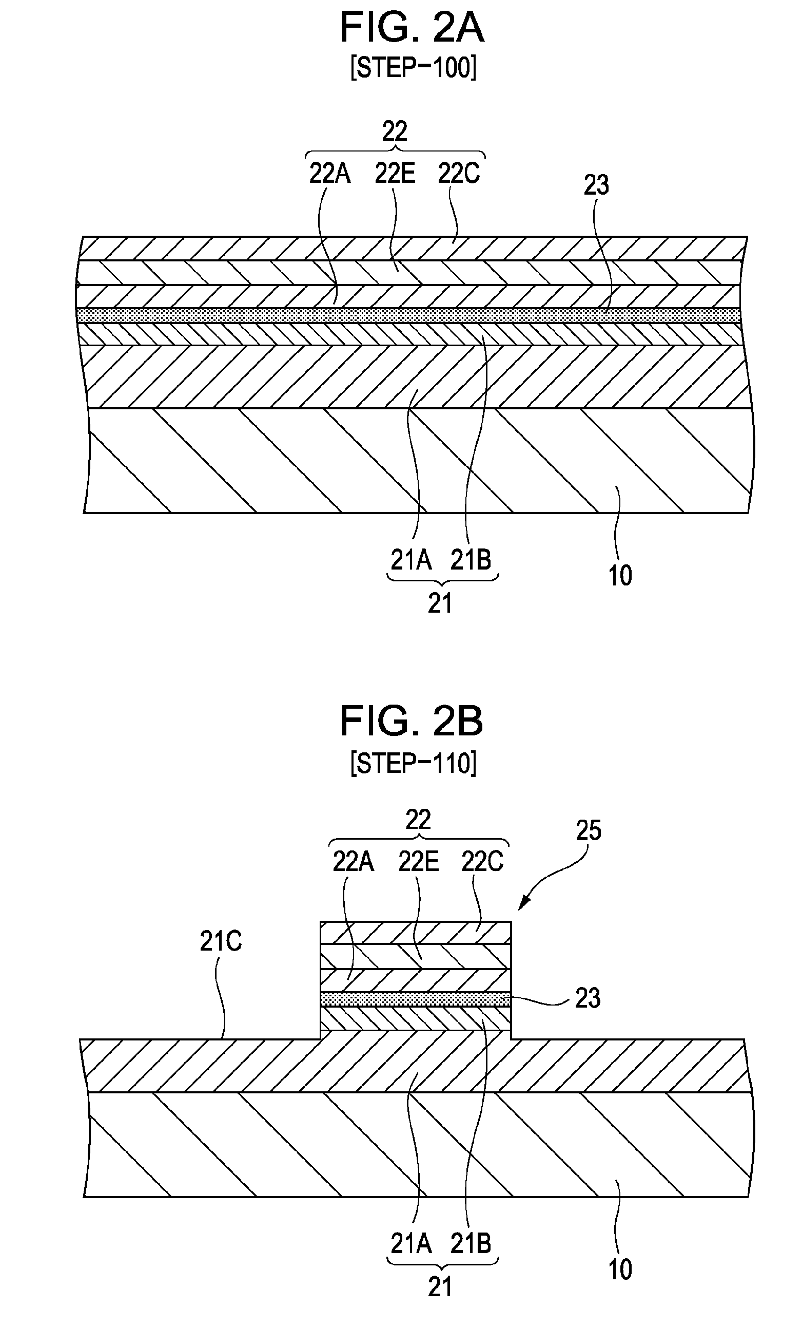
[0059]Example 1 relates to a light-emitting element assembly according to an embodiment of the present invention, and specifically to a light-emitting element assembly with a first configuration, and further relates to a method for manufacturing a light-emitting element assembly according to a first embodiment of the present invention. In Example 1 and Examples 2 and 3 described below, a first conductivity type is n-type, and a second conductivity type is p-type. In Example 1 and Examples 2 and 3 described below, a light-emitting element is a surface emitting laser element (vertical cavity surface emitting laser element, VCSEL) in which light is emitted through a first compound semiconductor layer.

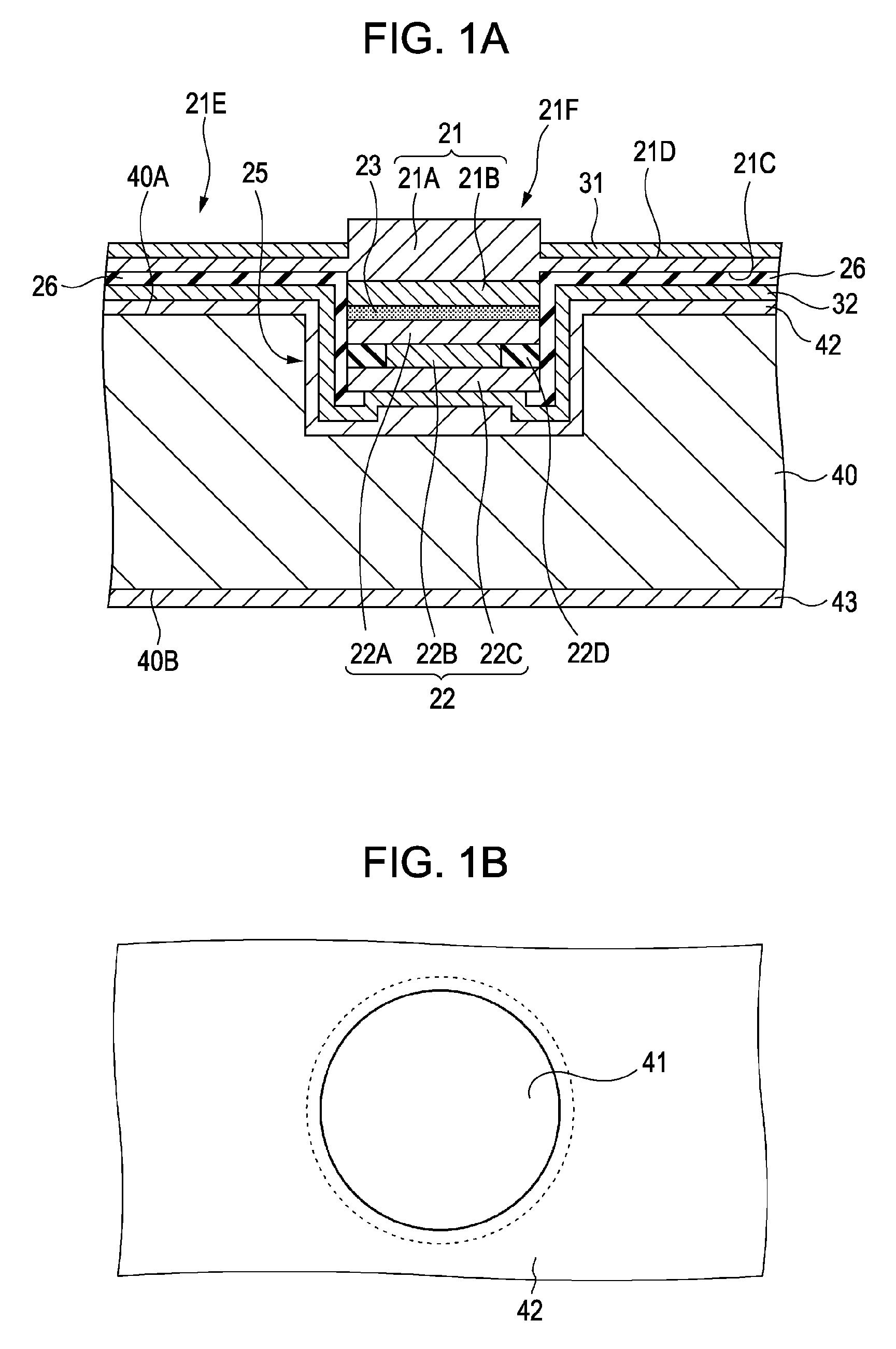
[0060]FIGS. 1A and 1B are a schematic partial sectional view of a light-emitting element assembly of Example 1 and a schematic partial plan view of a support substrate, respectively. The light-emitting element assembly of Example 1 is provided with a support substrate 40 and a light-emitti...

example 2

[0078]Example 2 is a modification of Example 1 and relates to a light-emitting element assembly having a second configuration.

[0079]As schematically shown in a partial sectional view of FIG. 8, in a light-emitting element assembly of Example 2, a first electrode 32 is not formed in a projective image of a mesa structure 25 along the axial direction of a recessed portion 41. In addition, unlike in Example 1, a first compound semiconductor layer 21 is not divided into first and second portions. The planar shape of the edge 31A of the first electrode 31 is the same as the shape of the projective image of the mesa structure 25.

[0080]Except for this point, the configuration and structure of the light-emitting element assembly of Example 2 may be the same as those of the light-emitting element assembly of Example 1. Therefore, detail description is omitted. In the light-emitting element assembly of Example 2, the first electrode 31 may be formed, on the basis of a so-called liftoff method...

example 3

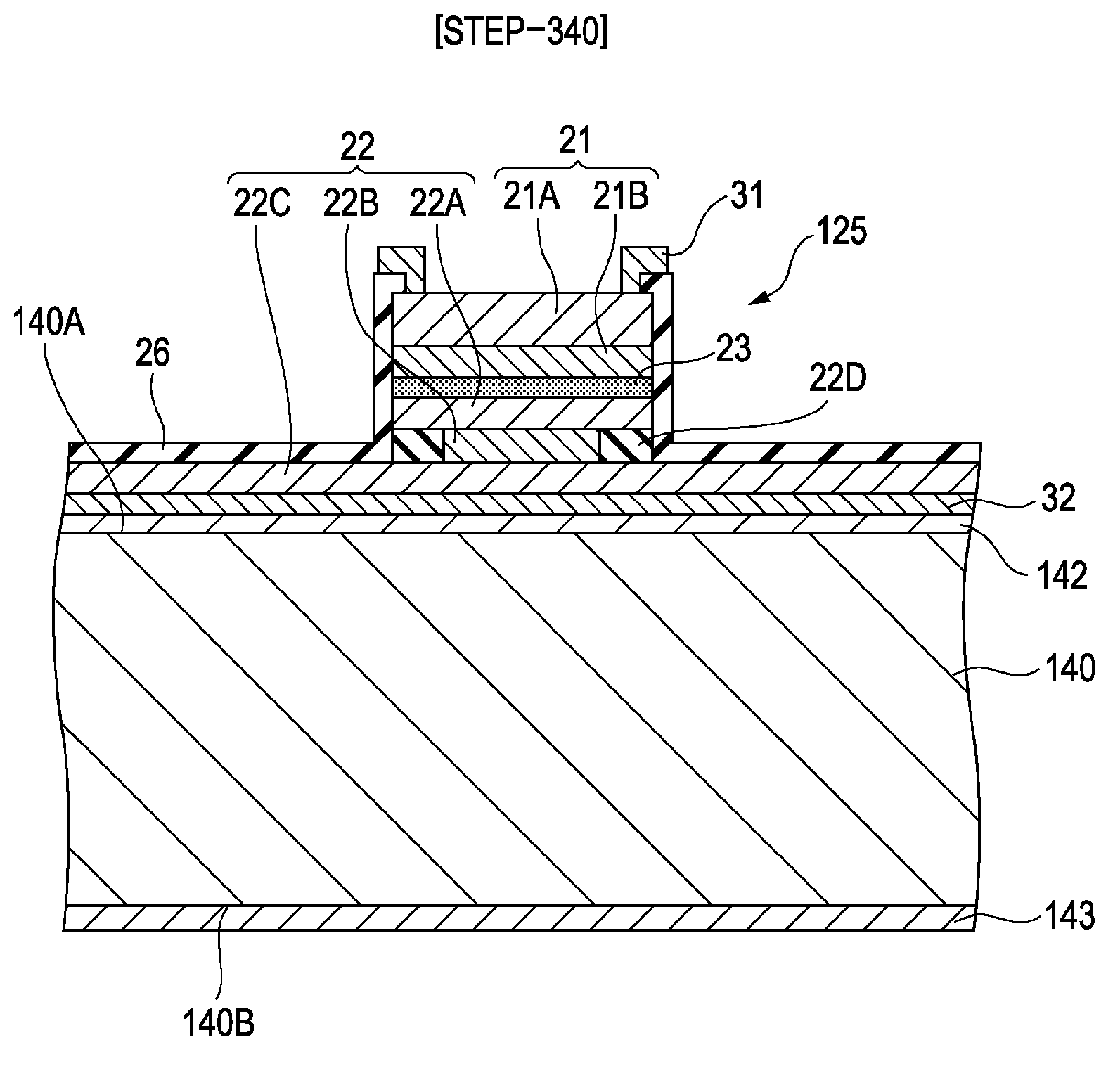
[0081]Example 3 relates to a method for manufacturing a light-emitting element assembly according to a second embodiment of the present invention. The method for manufacturing the light-emitting element of Example 3 is outlined with reference to FIGS. 9, 10, 11, 12, and 13 which are schematic partial sectional views of a laminated structure, etc.

Step-300

[0082]First, in the same manner as in Step-100 of Example 1, an etching stop layer (not shown), a first compound semiconductor layer 21 (a first DBR layer 21A and a first cladding layer 21B) of a first conductivity type (specifically, n type), a light-emitting portion (active layer) 23, and a second compound semiconductor layer 22 (a lower layer (second cladding layer) 22A, an intermediate layer 22E, and an upper layer (second DBR layer)22C) of a second conductivity type (specifically, p type) are deposited in order on a main surface of a n-GaAs substrate 10 for manufacturing a light-emitting element by a MOCVD technique. Further, a ...


PUM


Abstract

A light-emitting element assembly includes a support substrate having a first surface, a second surface facing the first surface, a recessed portion, and a conductive material layer formed over the first surface and the inner surface of the recessed portion, and a light-emitting element. The light-emitting element has a laminated structure including a first compound semiconductor layer, a light-emitting portion, and a second compound semiconductor layer, at least the second compound semiconductor layer and the light-emitting portion constituting a mesa structure. The light-emitting element further includes an insulating layer formed, a second electrode, and a first electrode. The mesa structure is placed in the recessed portion so that the conductive material layer and the second electrode are in at least partial contact with each other, and light emitted from the light-emitting portion is emitted from the second surface side of the first compound semiconductor layer.

Description

CROSS REFERENCES TO RELATED APPLICATIONS[0001]The present invention contains subject matter related to Japanese Patent Application JP 2007-334254 filed in the Japanese Patent Office on Dec. 26, 2007, the entire contents of which are incorporated herein by reference.BACKGROUND OF THE INVENTION[0002]1. Field of the Invention[0003]The present invention relates to a light-emitting element assembly and a method for manufacturing the same.[0004]2. Description of the Related Art[0005]In a surface emitting laser element, for example, an active layer having a multiquantum well structure is provided in a cavity held between two mirror layers (Distributed Bragg Reflector layers, DBR layers) which are provided on a substrate in the thickness direction thereof, and light emitted from the active layer (light-emitting portion) due to current injection is enclosed to cause laser oscillation. Such a surface emitting laser element uses a cylindrical mesa structure as disclosed in, for example, Japane...

Claims


Application Information

Patent Timeline
Patent Type & Authority Applications(United States)
IPC IPC(8): H01S5/026H01L21/02
CPCH01L33/0079H01L33/44H01L33/62H01L33/647H01S5/0207H01S5/0215H01S5/0216H01L2924/0002H01S5/0217H01S5/02272H01S5/0425H01S5/18311H01L2924/00H01L33/0093H01S5/0237
Inventor KODA, RINTAROARAKIDA, TAKAHIROTANIGUCHI, SATOSHIMASUI, YUJISUZUKI, NOBUHIROOKI, TOMOYUKIUCHIYAMA, CHIYOMIKIKUCHI, KAYOKO
Owner SONY CORP
Why Eureka
Try Eureka