Semiconductor device and its manufacturing method

a semiconductor and manufacturing method technology, applied in the field of laser irradiation, can solve problems such as restricted layou

Active Publication Date: 2009-07-09
SEMICON ENERGY LAB CO LTD
View PDF99 Cites 27 Cited by
  • Summary
  • Abstract
  • Description
  • Claims
  • Application Information

AI Technical Summary

Benefits of technology

[0014]As thus described, the top-flat distribution has advantages. However, the technique using a diffractive optical element has some problems of technical difficulty and high cost because the diffractive optical element needs a microscopic process with the accuracy in units of nanometer in order to obtain high characteristic. The technique using an optical waveguide also has a problem of interference fringes appearing on the irradiation surface due to the high and low intensity of the laser beam because the laser beam having a wavelength of 532 nm has coherency to the semiconductor film.
[0016]In view of the above problems, it is an object of the present invention to provide a laser irradiation apparatus which can decrease the proportion of the microcrystal region in the whole region irradiated with the laser beam and which can conduct a laser process to the semiconductor film homogeneously.
[0025]According to the present invention, a laser irradiation apparatus can be provided which can suppress the one width of the microcrystal region in the laser irradiation region to 1 to 20 μm and which can conduct a laser process to a semiconductor film homogeneously when the semiconductor film is crystallized with a laser.

Problems solved by technology

In such a case, it is apparent that the layout is restricted.

Method used


Image

  • Semiconductor device and its manufacturing method
  • Semiconductor device and its manufacturing method
  • Semiconductor device and its manufacturing method

Examples


embodiment 1

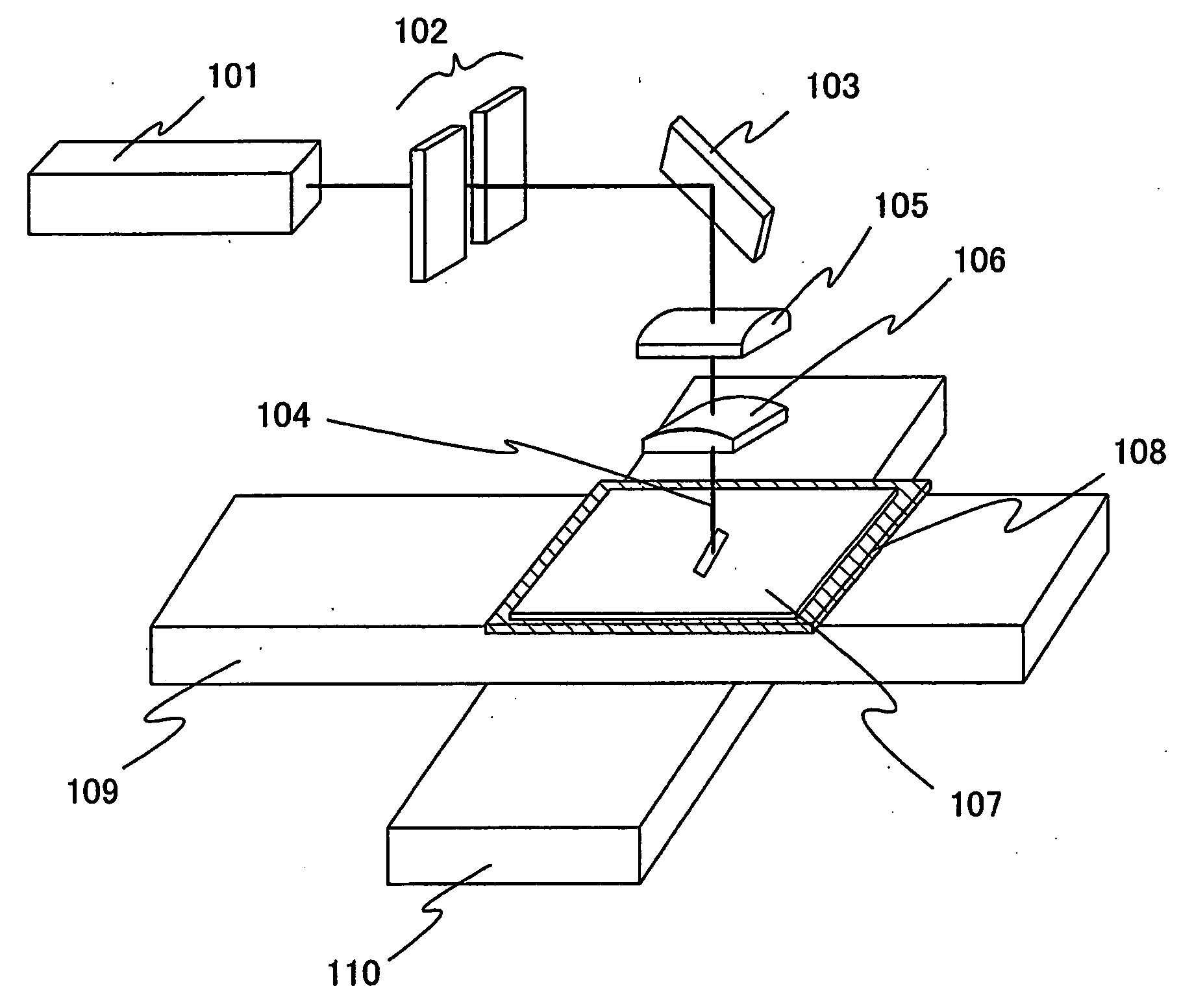
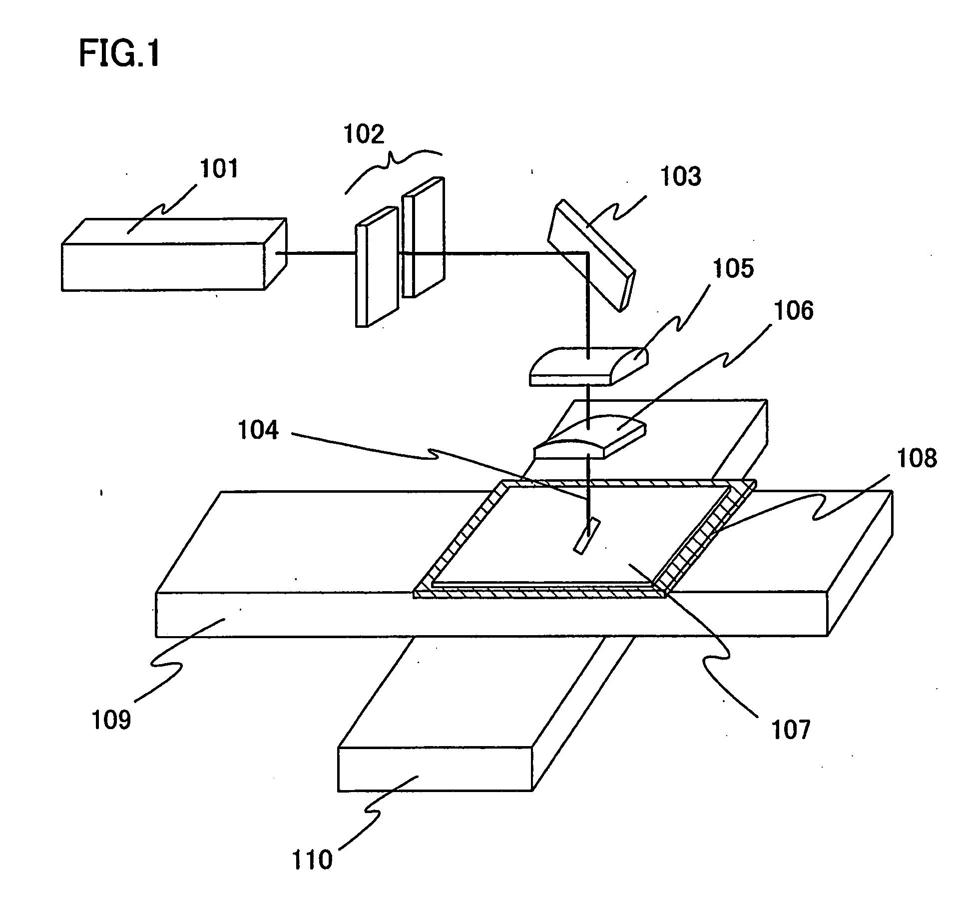
[0075]This embodiment describes the first laser irradiation method and apparatus in which a laser beam whose low-intensity portion has been blocked enters an irradiation surface perpendicularly. Since the same drawings as those in Embodiment Mode are used in this embodiment, the same element is denoted with the same reference numeral.

[0076]The laser oscillator 101 in FIG. 1 is a mode-locked pulsed laser oscillator having an output power of 10 W, a repetition rate of 80 MH, a pulse width of 10 ps, a wavelength of 532 nm, a beam diameter of 1.0 mm, and TEM00 mode (single transverse mode). The mode-locked pulsed laser used here has the repetition rate which is extremely higher than a repetition rate of several tens to several hundred Hz of a conventional pulsed laser. It is said that it takes several tens to several hundred ns to completely solidify the semiconductor film after irradiating the semiconductor film with a pulsed laser beam. With the pulsed laser oscillator having a repeti...

embodiment 2

[0086]In this embodiment, two CW lasers are used. After laser beams emitted from these two CW lasers are combined, the combined laser beam passes through an optical system of the present invention and is delivered.

[0087]In FIG. 4, lasers 401 and 402 are known CW lasers. For example, a CW solid-state laser such as a laser having a medium of a single-crystal YAG, YVO4, forsterite (Mg2SiO4), YAlO3, or GdVO4, or a poly-crystal YAG, Y2O3, YVO4, YAlO3, or GdVO4, each of which is doped with one or a plurality of Nd, Yb, Cr, Ti, Ho, Er, Tm, and Ta as dopant, an alexandrite laser, or a Ti:sapphire laser can be used. Moreover, a CW semiconductor laser such as a GaN laser, a GaAs laser, or an InAs laser, or a CW gas laser such as an Ar laser can be used.

[0088]Laser beams emitted from the lasers 401 and 402 are converted into harmonics by a known non-linear optical element such as BBO, LBO, KTT, KDP, LiNbO3, LiIO3, CLBO, ATP, BIBO, or KB5. Since the semiconductor laser is pumped by emitting lig...

embodiment 3

[0103]This embodiment describes an example of manufacturing a peelable dual-gate TFT with the use of a semiconductor film crystallized by using a laser irradiation apparatus of the present invention.

[0104]As shown in FIG. 6A, a metal film 602, an oxide film containing a metal element in the metal film 602 (this oxide film is hereinafter referred to as a metal oxide film 603), and a silicon oxide film 604 are formed in order over a first substrate 601 having an insulating surface. The first substrate 601 may be any substrate as long as the substrate can resist the following steps. For example, a glass substrate, a quartz substrate, a ceramic substrate, a silicon substrate, a metal substrate, or a stainless steel substrate can be used.

[0105]In this embodiment, W (tungsten) is used for the metal film 602. Alternatively, the metal film 602 can be formed with metal selected from Ti, Ta, Mo, Nd, Ni, Co, Zr, Zn, Ru, Rh, Pd, Os, and Ir, an alloy material containing any one of these elements...


PUM

PropertyMeasurementUnit
widthaaaaaaaaaa
thicknessaaaaaaaaaa
lengthaaaaaaaaaa

Abstract

It is an object of the present invention to provide laser irradiation apparatus and method which can decrease the proportion of the microcrystal region in the whole irradiated region and can irradiate a semiconductor film homogeneously with a laser beam. A low-intensity part of a laser beam emitted from a laser oscillator is blocked by a slit, the laser beam is deflected by a mirror, and the beam is shaped into a desired size by using two convex cylindrical lenses. Then, the laser beam is delivered to the irradiation surface.

Description

1. TECHNICAL FIELD[0001]The present invention relates to a laser irradiation apparatus (an apparatus including a laser and an optical system for guiding a laser beam emitted from the laser to an irradiation object) and a laser irradiation method, which anneal a semiconductor material or the like homogeneously and effectively. The present invention further relates to a semiconductor device manufactured by including a step of the laser process and to its manufacturing method.2. BACKGROUND ART[0002]In recent years, a technique to form a thin film transistor (hereinafter referred to as a TFT) over a substrate has made great progress and application to an active matrix display device has been advanced. In particular, a TFT formed using a poly-crystalline semiconductor film is superior in field-effect mobility to a TFT formed using a conventional amorphous semiconductor film; therefore, high-speed operation has become possible. For this reason, it is tried that a pixel, which has been con...

Claims


Application Information

Patent Timeline
Patent Type & Authority Applications(United States)
IPC IPC(8): B23K26/00H01L21/36H01L21/428
CPCB23K26/0604B23K26/066H01L21/268H01L27/1296H01L29/78621H01L29/78648H01L2029/7863
Inventor TANAKA, KOICHIROISOBE, ATSUOYAMAMOTO, YOSHIAKI
Owner SEMICON ENERGY LAB CO LTD
Why Eureka
Try Eureka