
Semiconductor device

a technology of semiconductor devices and control signals, applied in the direction of generating/distributing signals, pulse techniques, instruments, etc., can solve the problems of increasing the variation of device characteristics incurred by miniaturization, shifting the trigger timing of a control signal, and reducing the dead margin of timing design. , the effect of reducing the dead margin

Active Publication Date: 2009-07-16
LONGITUDE LICENSING LTD
View PDF2 Cites 17 Cited by
  • Summary
  • Abstract
  • Description
  • Claims
  • Application Information

AI Technical Summary

Benefits of technology

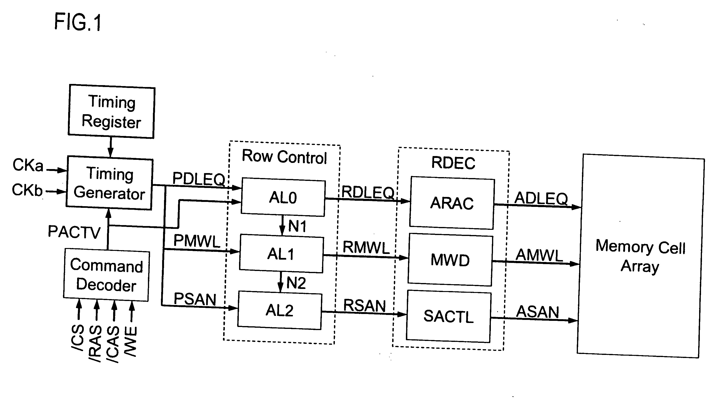
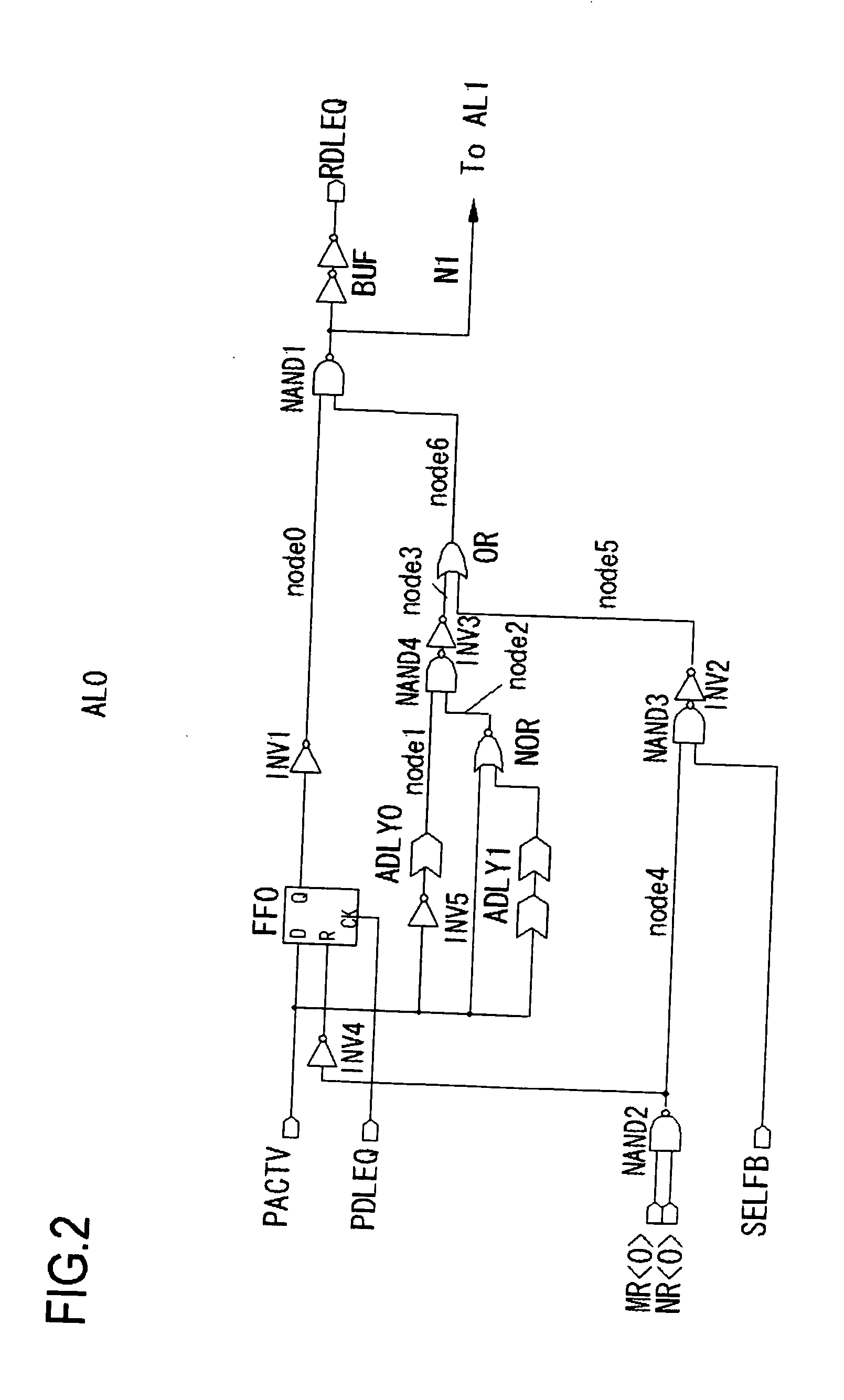
[0027]As described above, the analog delay ADLY0 is an adjustment circuit for making adjustment so that deactivation of a precharging circuit and word line activation will occur at approximately the same time. That is, the analog delay adjusts the precharge-word line margin tDEQWLM_B so that it will be of a necessary minimum value. In similar manner, the delay time of the analog delay ADLY1 is adjusted so that the outputting of the read signal will occur approximately at the same time as activation of the sense amplifier circuit. That is, adjustment id made so that the word line-sense amplifier margin tWLSAM_B will be of a necessary minimum value. Timing designing is made in this manner so that the timing margin between respective timing signals will be reduced to as small a value as possible to provide for short access time.
[0040]The use of the digital delay circuit gives rise to a merit that, since the delay determined by the period of the clock supplied from outside may be produced, changes in the delay amount is small even though the devices, temperature or power supply voltages are changed.
[0042]However, the driving current for a DLL is high so that the power consumption during chip operation is increased. In addition, with the DLL, a certain time (approximately 100 cycles) has to pass as from clock delivery until the internal delay is synchronized with the clock. Hence, the clock cannot be halted even in the standby mode of the DRAM, with the result that current consumption for the standby mode is increased.
[0061]According to the present invention, a semiconductor device may be provided in which timing variations are little against changes in power supply voltage or temperature. The present invention may be applied to a semiconductor memory, such as DRAM, to reduce the dead margin in timing designing to enable high speed access or low power consumption.

Problems solved by technology

However, as the memory cell miniaturization advances through 65 nm nodes and 45 nm nodes, a variety of side effects come out, even though the aforementioned merits of higher performance may be achieved.
The principal side effect is increased variations of device characteristics incurred by miniaturization.
In particular, variations in a threshold voltage of a transistor may cause shifting of a trigger timing of a control signal within a DRAM chip.
This shifting in a trigger timing of a control signal may, in turn, cause mistaken operations of the DRAMs.
That is, the variations in the threshold voltage value severely affect the yield of the chip.
Variations in device characteristics pose a serious problem as a result of recent progress in the use of lower voltage as external power supplies and due to manufacture tolerances of MOS transistors or interconnects in an LSI brought about by miniaturization.

Method used


Image

  • Semiconductor device
  • Semiconductor device
  • Semiconductor device

Examples


Embodiment Construction

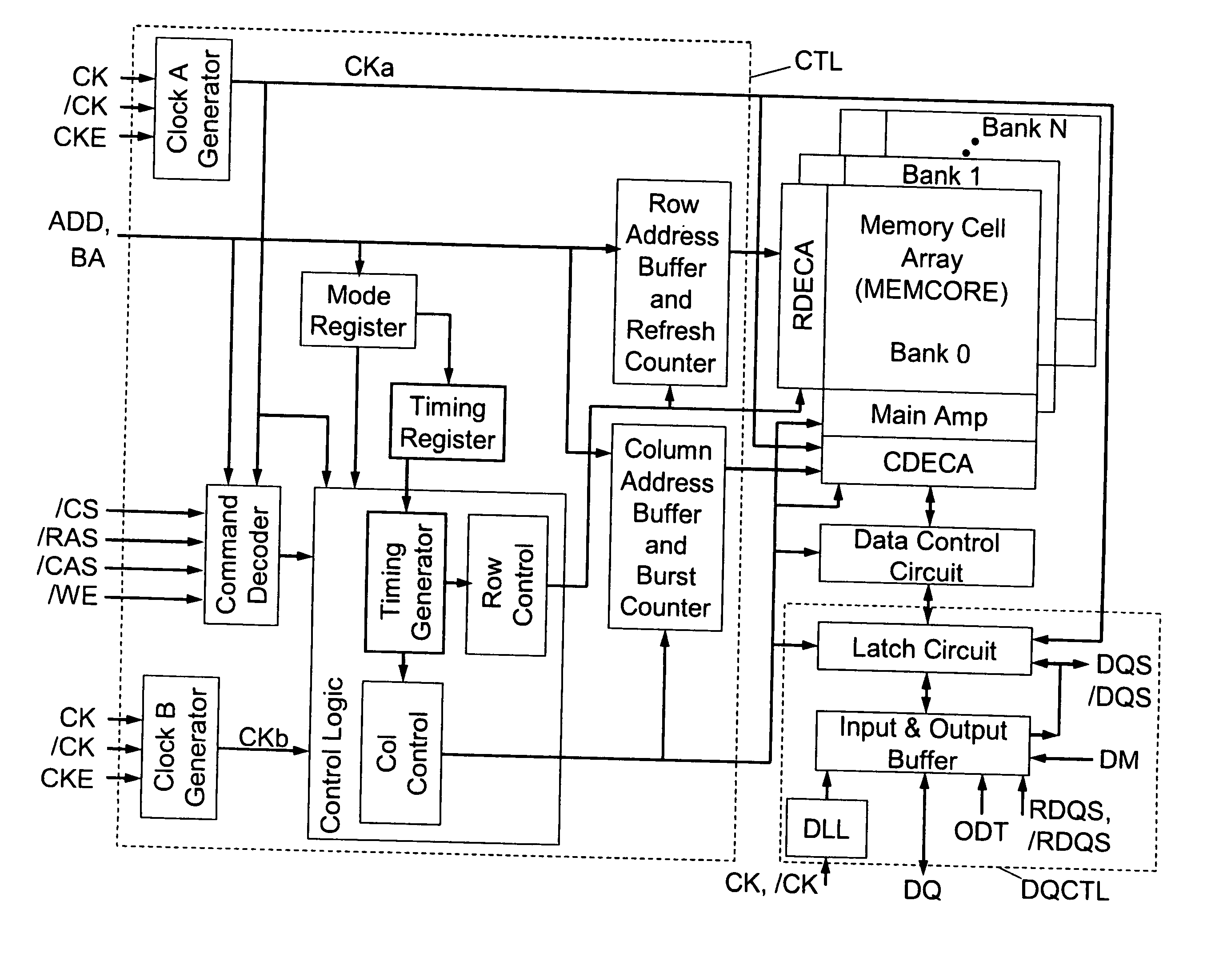
[0102]Exemplary embodiments of the present invention will now be described with reference to the drawings. In all figures referred to in the following description, the same reference numerals or symbols are used to depict the same parts of components, as a principle, and repetition of description of the same or similar parts or components is dispense with.

[0103]According to an exemplary embodiment of the present invention, there are provided a first clock generating circuit (Clock A Generator) that generates a first clock signal CKa having a first period T1, a second clock generating circuit (Clock B Generator) that generates a second clock signal CKb having a second period T2, and a timing generator. The timing generator receives the first clock CKa, the second clock CKb and an activation signal (PACTV) and generates a timing signal at a timing of delay time of td=m·T1+n·T2 from the time of activation of the activation signal (PACTV), where m and n are non-negative integers that pr...


PUM


Abstract

Disclosed is a semiconductor device including a first clock generator that generates a first clock signal having a first period from an input clock signal, a second clock generator that generates a second clock signal having a second period from the input clock signal, and a timing generator that receives the first clock signal, the second clock signal, an activation signal from a command decoder and a selection signal for selecting the delay time from a timing register to produce a timing signal delayed as from activation of the activation signal by a delay equal to a sum of a time equal to a preset number m prescribed by the selection signal times the first period and a time equal to another preset number n prescribed by the selection signal times the second period. The timing register holds the values of m and n. These values are set in the timing register in an initialization sequence at the time of a mode register set command. In the operating states, the timing signals are output from the timing generator at a desired timing based on the information stored in the timing register (FIG. 6).

Description

REFERENCE TO RELATED APPLICATION[0001]This application is based upon and claims the benefit of the priority of Japanese patent application No. 2007-326220 filed on Dec. 18, 2007, the disclosure of which is incorporated herein in its entirety by reference thereto.FIELD OF THE INVENTION[0002]This invention relates to a semiconductor device. More particularly, it relates to timing control within a chip of a semiconductor memory of high speed and high integration or a chip of a semiconductor device integrated from a logic circuit and a semiconductor memory.DESCRIPTION OF RELATED ART[0003]A large number of dynamic random access memories (Dynamic Random Access Memories, abbreviated below to DRAMs), are mounted in a wide variety of electronic equipments. In keeping up with recent needs to low power consumption and to high performance of electronic equipments, there is a strong demand for high performance, such as low power consumption, high operating speed and large capacity of DRAMs mount...

Claims


Application Information

Patent Timeline
Patent Type & Authority Applications(United States)
IPC IPC(8): G11C7/00H03L7/06G11C8/18G06F1/04G11C11/4076H01L21/8242H01L27/108H03K5/00H03K5/13H03K5/131H03K19/0175
CPCH01L27/108H01L27/10897H03K5/15066G11C7/1048H01L27/0207G11C7/20G11C7/22G11C7/222G11C11/4094G11C7/12G11C7/04H10B12/00H10B12/50
Inventor IDE, AKIRATAKAI, YASUHIROSEKIGUCHI, TOMONORITAKEMURA, RIICHIROAKIYAMA, SATORUNAKAYA, HIROAKI
Owner LONGITUDE LICENSING LTD
Learn More