Semiconductor sensor and method for manufactruing the same

a technology of semiconductors and sensors, applied in the field of semiconductor sensors, can solve the problems of increasing the manufacturing cost and the price of chemical sensors, and achieve the effects of low price, high sensitivity, and easy growth of ridge-and-valley portions

Active Publication Date: 2009-07-23
SEIKO EPSON CORP
View PDF2 Cites 12 Cited by
  • Summary
  • Abstract
  • Description
  • Claims
  • Application Information

AI Technical Summary

Benefits of technology

[0007]An advantage of the invention is to provide a semiconductor sensor having a high sensitivity with a low price, and a method for manufacturing the semiconductor sensor.
[0008]According to a first aspect of the invention, a semiconductor sensor includes: a semiconductor substrate; a plurality of piezoelectric thin films layered on the semiconductor substrate, the plurality of piezoelectric thin films including at least a pair of the piezoelectric thin films layered above and below; a pair of electrodes that are formed at an interface of at least the pair of the piezoelectric thin films and excite surface acoustic waves; a thin film directly under a lowest-layer piezoelectric film of the piezoelectric thin films; a metal thin film that is formed at an interface of the lowest-layer piezoelectric thin film and the thin film, and facilitate a growth of a ridge-and-valley portion on a surface of an uppermost-layer piezoelectric thin film of the piezoelectric thin films; and a sensitive film for molecular adsorption formed on at least the ridge-and-valley portion on the uppermost-layer piezoelectric thin film.
[0009]In the semiconductor sensor, the metal thin film formed at the interface of the lowest-layer piezoelectric thin film and the thin film directly under the lowest-layer piezoelectric thin film can produce the ridge-and-valley portion on the surface of the uppermost-layer piezoelectric thin film. That is, the surface area of the sensitive film for molecular adsorption formed on the surface of the uppermost-layer piezoelectric thin film (i.e., molecular adsorption area) can be enlarged, providing a semiconductor sensor having a high sensitivity. In addition, the metal thin film can be formed by using conventional semiconductor manufacturing processes without employing a particular process for enlarging the surface area of the sensitive film as necessary in related art, e.g., JP-A-2007-147556. Thus, the manufacturing costs can be reduced. Consequently, a semiconductor sensor having a high sensitivity can be provided with low price.
[0010]In the sensor, the metal thin film is preferably a metal facilitating a crystal growth of a wurtzite structure of the piezoelectric thin films in a c-axis direction.
[0011]The metal can facilitate the growth of the ridge-and-valley portion on the surface of the uppermost-layer piezoelectric thin film.
[0012]In addition, it is preferable that any one of Pt, Au, Al, Ag, Cu, Mo, Cr, Nb, W, Ni, Fe, Ti, Co, Zn, and Zr be used for the metal thin film.

Problems solved by technology

The related art described above has a problem in that such particular steps are additionally required in order to improve the adsorption sensitivity of the sensitive film, increasing the manufacturing costs and the price of the chemical sensor.

Method used


Image

  • Semiconductor sensor and method for manufactruing the same
  • Semiconductor sensor and method for manufactruing the same
  • Semiconductor sensor and method for manufactruing the same

Examples


first embodiment

[0045]Semiconductor Sensor

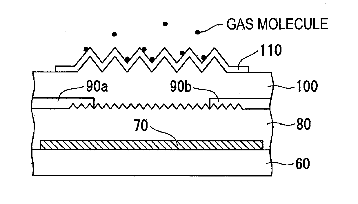
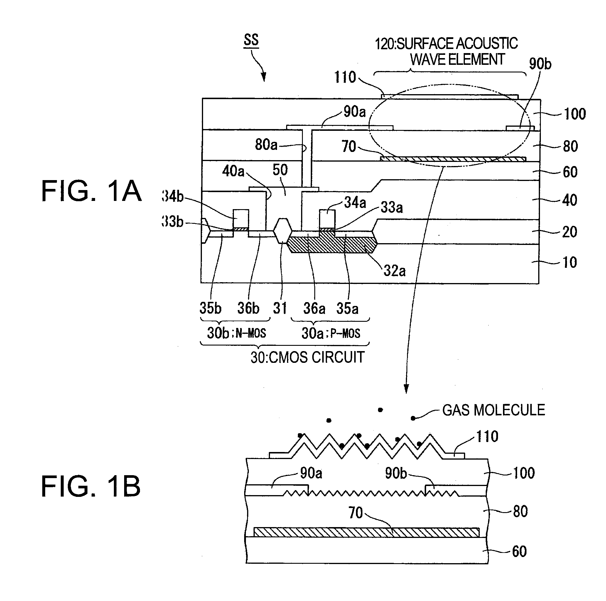
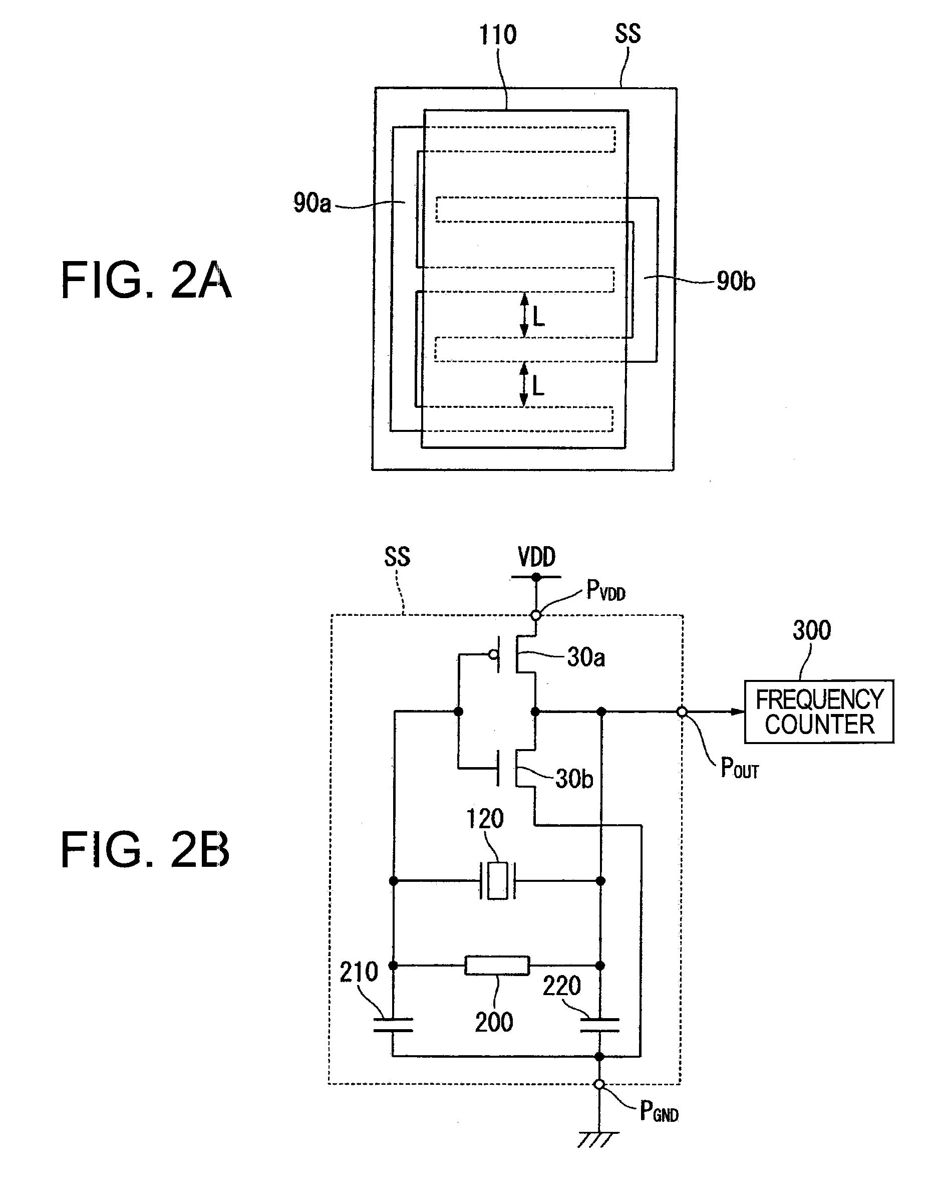
[0046]FIG. 1A is a sectional view illustrating a semiconductor sensor SS according to a first embodiment of the invention. FIG. 1B is a detailed view of a portion of the semiconductor sensor SS shown in FIG. 1A. FIG. 2A is a top view of the semiconductor sensor SS. FIG. 2B is an equivalent circuit diagram of the semiconductor sensor SS.

[0047]As shown in FIG. 1A, the semiconductor sensor SS of the first embodiment includes a semiconductor substrate 10, a local oxidization of silicon (LOCOS) film 20, a complementary metal oxide semiconductor (CMOS) circuit 30, a first interlayer film 40, a CMOS output electrode 50, a second interlayer film 60, a metal thin film 70, a first piezoelectric thin film 80, a first electrode 90a, a second electrode 90b, a second piezoelectric thin film 100, and a sensitive film 110. The metal thin film 70, the first piezoelectric thin film 80, the first electrode 90a, the second electrode 90b, the second piezoelectric thin film 100 ...

second embodiment

[0060]Method for Manufacturing a Semiconductor Sensor

[0061]A method for manufacturing the semiconductor sensor SS according to a second embodiment of the invention is described with reference to FIGS. 3A to 8B.

[0062]First, the CMOS circuit forming region and the surface acoustic wave element forming region are electrically separated on the semiconductor substrate 10 by using a LOCOS separation method. As shown in FIG. 3A, a silicon nitride film (SiNx) 11 is deposited on the semiconductor substrate 10 (P-type Si substrate) by using a CVD method. Then, as shown in FIG. 3B, the silicon nitride film 11 in the CMOS circuit forming region is left while the silicon nitride film 11 in the surface acoustic wave element forming region is removed (etched) by patterning the silicon nitride film 11 with a photolithography method. Next, as shown in FIG. 3C, a silicon oxide film (the LOCOS film 20) is formed by oxidizing, at a high temperature, a region from which the silicon nitride film 11 has b...


PUM

PropertyMeasurementUnit
thicknessaaaaaaaaaa
temperatureaaaaaaaaaa
thicknessaaaaaaaaaa

Abstract

A semiconductor sensor includes: a semiconductor substrate; a plurality of piezoelectric thin films layered on the semiconductor substrate, the plurality of piezoelectric thin films including at least a pair of the piezoelectric thin films layered above and below; a pair of electrodes that are formed at an interface of at least the pair of the piezoelectric thin films layered above and below and excite surface acoustic waves; a thin film directly under a lowest-layer piezoelectric film of the piezoelectric thin films; a metal thin film that is formed at an interface of the lowest-layer piezoelectric thin film and the thin film, and facilitate a growth of a ridge-and-valley portion on a surface of an uppermost-layer piezoelectric thin film of the piezoelectric thin films; and a sensitive film for molecular adsorption formed on at least the ridge-and-valley portion on the uppermost-layer piezoelectric thin film.

Description

BACKGROUND[0001]1. Technical Field[0002]The present invention relates to a semiconductor sensor and a method for manufacturing the semiconductor sensor.[0003]2. Related Art[0004]Recently, chemical sensors, odor sensors, gas sensors, and the like that detect chemical substances in the air have been developed in response to increasing awareness of environmental issues. In the sensors, a sensitive film on which chemical substances adsorb is formed on a piezoelectric element, such as a quartz crystal resonator and a surface acoustic wave element, and the mass change of the sensitive film corresponds to the oscillation frequency change of the piezoelectric element. As a result, the chemical substances can be detected by using the mass change.[0005]For example, JP-A-2007-147556 discloses a method for manufacturing a thin film (sensitive film) and a chemical sensor using the thin film manufactured by the method. In order to improve adsorption sensitivity (i.e., the sensitivity of the senso...

Claims


Application Information

Patent Timeline
Patent Type & Authority Applications(United States)
IPC IPC(8): G01N37/00H01L41/04H01L41/22H01L21/02G01N5/02
CPCY10T29/42G01N5/02
Inventor TAKIZAWA, TERUOKONDO, TAKAYUKITODOROKIHARA, MASAYOSHI
Owner SEIKO EPSON CORP
Why Eureka
Try Eureka