ESD/EOS Performance by Introduction of Defects

Active Publication Date: 2009-07-23
INFINEON TECH AG
View PDF11 Cites 17 Cited by
  • Summary
  • Abstract
  • Description
  • Claims
  • Application Information

AI Technical Summary

Benefits of technology

[0009]In accordance with an exemplary embodiment, an avalanche diode is provided. The avalanche diode can be coupled, without limitation, to an external circuit node in an electronic system to provide ESD/EOS protection for the circuit node. The avalanche diode includes an anode region, a cathode region adjoining the anode region, and an avalanche ignition region formed in a region surrounding juncture of the anode region with the cathode region. The avalanche ignition region is formed with an enhanced defect concentration level over a defect concentration level of the anode region and/or the cathode region. In an advantageous embodiment, the avalanche

Problems solved by technology

In particular, many integrated circuits and semiconductor devices are highly susceptible to damage from the unintended discharge of static electricity, generally as a result of handling or from physical contact with another charged body, or from electrical overstress.
These events have become a critical problem for the electronics industry.
Often, the device is only slightly weakened but is less able to withstand normal operating stresses and, hence, may result in a reliability problem.
When an ESD discharge or EOS event is coupled to a transistor or other semiconductor element, the high vol

Method used


Image

  • ESD/EOS Performance by Introduction of Defects
  • ESD/EOS Performance by Introduction of Defects
  • ESD/EOS Performance by Introduction of Defects

Examples


Example

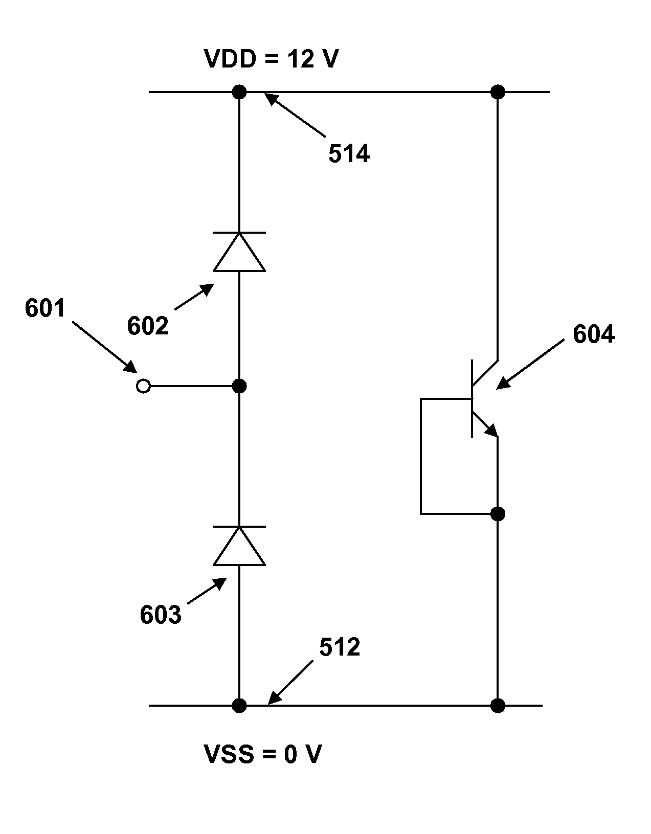
[0017]The making and using of the presently preferred embodiments are discussed in detail below. It should be appreciated, however, that the present invention provides many applicable inventive concepts that can be embodied in a wide variety of specific contexts. The specific embodiments discussed are merely illustrative of specific ways to make and use the invention, and do not limit the scope of the invention.

[0018]The present invention will be described with respect to exemplary embodiments in a specific context, namely an ESD / EOS protection arrangement including a semiconductor device. The semiconductor device includes a depletion region with an enhanced level of defects to provide rapid onset of an avalanche condition. The invention may also be applied, however, to other semiconductor structures, and is not limited to this particular implementation. Other integrated circuits can be protected from ESD / EOS discharges in different contexts using inventive concepts described herein...


PUM


Abstract

The invention relates to an avalanche diode that can be employed as an ESD protection device. An avalanche ignition region is formed at the p-n junction of the diode and includes an enhanced defect concentration level to provide rapid onset of avalanche current. The avalanche ignition region is preferably formed wider than the diode depletion zone, and is preferably created by placement, preferably by ion implantation, of an atomic specie different from that of the principal device structure. The doping concentration of the placed atomic specie should be sufficiently high to ensure substantially immediate onset of avalanche current when the diode breakdown voltage is exceeded. The new atomic specie preferably comprises argon or nitrogen, but other atomic species can be employed. However, other means of increasing a defect concentration level in the diode depletion zone, such as an altered annealing program, are also contemplated.

Description

TECHNICAL FIELD[0001]An embodiment of the invention relates generally to integrated circuits, semiconductor devices, and methods, and more particularly to ESD (electrostatic discharge) and EOS (electrical overstress) protection devices with an enhanced level of defects and method of protecting an integrated circuit against electrostatic discharge and electrical overstress.BACKGROUND[0002]As electronic circuits continue to become smaller and are widely applied in unprotected environments, it has become easier to either completely destroy or otherwise impair electronic components therein by application of voltages beyond component ratings. In particular, many integrated circuits and semiconductor devices are highly susceptible to damage from the unintended discharge of static electricity, generally as a result of handling or from physical contact with another charged body, or from electrical overstress. Electrostatic discharge is the transfer of an electric charge between bodies at di...

Claims


Application Information

Patent Timeline
IPC IPC(8): H02H9/00H01L29/866H01L21/329
CPCH01L23/62H01L27/0255H01L29/32H01L29/861H01L29/866H01L2924/0002H01L29/66113H01L29/7302H01L2924/00H01L21/26506H01L21/3221H01L27/0259H01L29/0603
Inventor SCHNEIDER, JENSESMARK, KAIWENDEL, MARTIN
Owner INFINEON TECH AG
Why Eureka
Try Eureka