On-track process for patterning hardmask by multiple dark field exposures

a technology of multiple exposure and hardmask, which is applied in the field of fabricating semiconductor structures by microphotolithography, can solve the problems of high cost and high unproven potential for small cds, and high cost and complexity of multiple exposure process

Active Publication Date: 2009-07-30
BREWER SCI
View PDF100 Cites 14 Cited by
  • Summary
  • Abstract
  • Description
  • Claims
  • Application Information

AI Technical Summary

Benefits of technology

[0014]The present invention also provides another inventive method of forming a microelectronic structure by applying a hardmask composition to the surface of a substrate. The hardmask composition comprises a polymer dispersed or dissolved in a solvent system. The composition is baked to form a hardmask layer on the substrate. A photosensitive composition is applied on the hardmask to form a first imaging layer on top of the hardmask layer, and the first imaging layer is exposed to activating radiation to yield exposed portions in the first imaging layer. The first imaging layer is contacted with a developer, so as to remove the exposed portions of the imaging layer. Advantageously, this also results in the removal of portions of the hardmask layer beneath the exposed portions in the first imaging layer, yielding a patterned hardmask layer. The first imaging layer is then contacted with an organic solvent to remove the first imaging layer from the patterned hardmask layer. A second photosensitive composition is applied to the patterned hardmask layer to form a second imaging layer on top of the patterned hardmask layer. This is accomplished without any dry etching occurring during the foregoing process.

Problems solved by technology

The potential for smaller CDs had not been seriously investigated until recently, primarily for two reasons: (1) the high cost and high complexity of the multiple exposure process, and (2) the availability of other options for CD reduction.
However, these options are quite costly and require new tool sets.
One drawback to the traditional bright field process is that a hardmask must be reapplied to the substrate before the second exposure-development-etching process.
This additional step increases processing time as well as overall cost.
The dry-etch step greatly complicates the double exposure technology.

Method used


Image

  • On-track process for patterning hardmask by multiple dark field exposures
  • On-track process for patterning hardmask by multiple dark field exposures
  • On-track process for patterning hardmask by multiple dark field exposures

Examples


example 1

Hardmask Formulation I

[0046]In this procedure a developer-soluble hardmask was formulated using the ingredients from Table 1. The ingredients were added to a flask in the order listed below and mixed under agitation. The mixture was filtered through a 0.1-micron membrane to remove particles. The formulation was then spin-coated onto a silicon wafer at 2,000 rpm for 40 seconds, followed by a two-stage bake at 120° C. for 40 seconds and then at 200° C. for 60 seconds. The thickness of the resulting film was measured to be about 75 nm±5 nm. The index of refraction of the film was measured to be about 1.6±0.05 at 193 nm, about 1.8±0.05 at 248 nm, and about 1.7±0.05 at 365 nm. The extinction coefficient of the film was measured to be about 0.38±0.05 at 193 nm, about 0.39±0.05 at 248 nm, and 0.42±0.05 at 365 nm.

[0047]The wafer was then immersed in TMAH while the analyzer measured the rate at which the film was removed. This film's dissolution rate in 0.26N TMAH was measured to be about 3 ...

example 2

Vias Created on Hardmask I by Double Exposure-Development

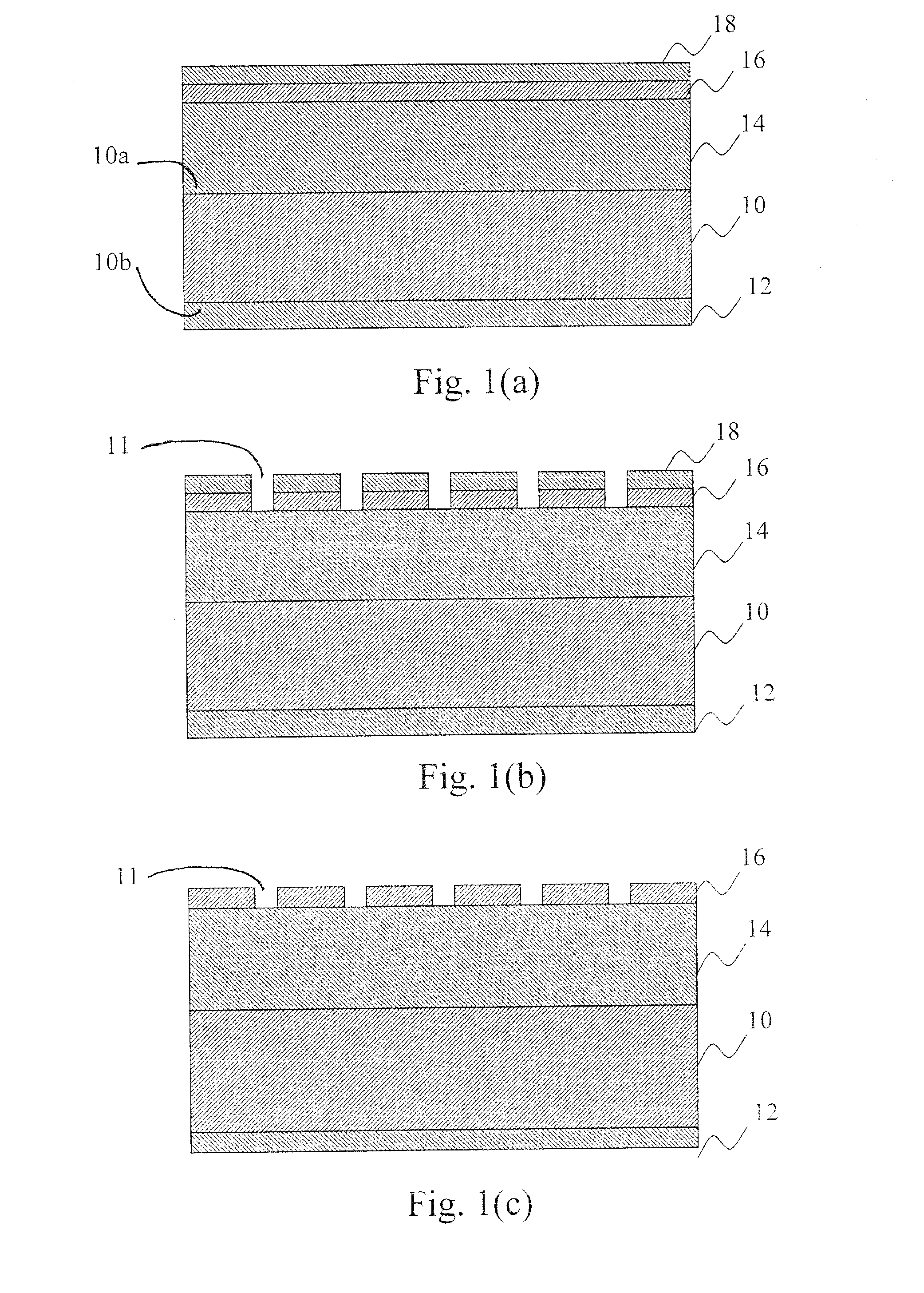
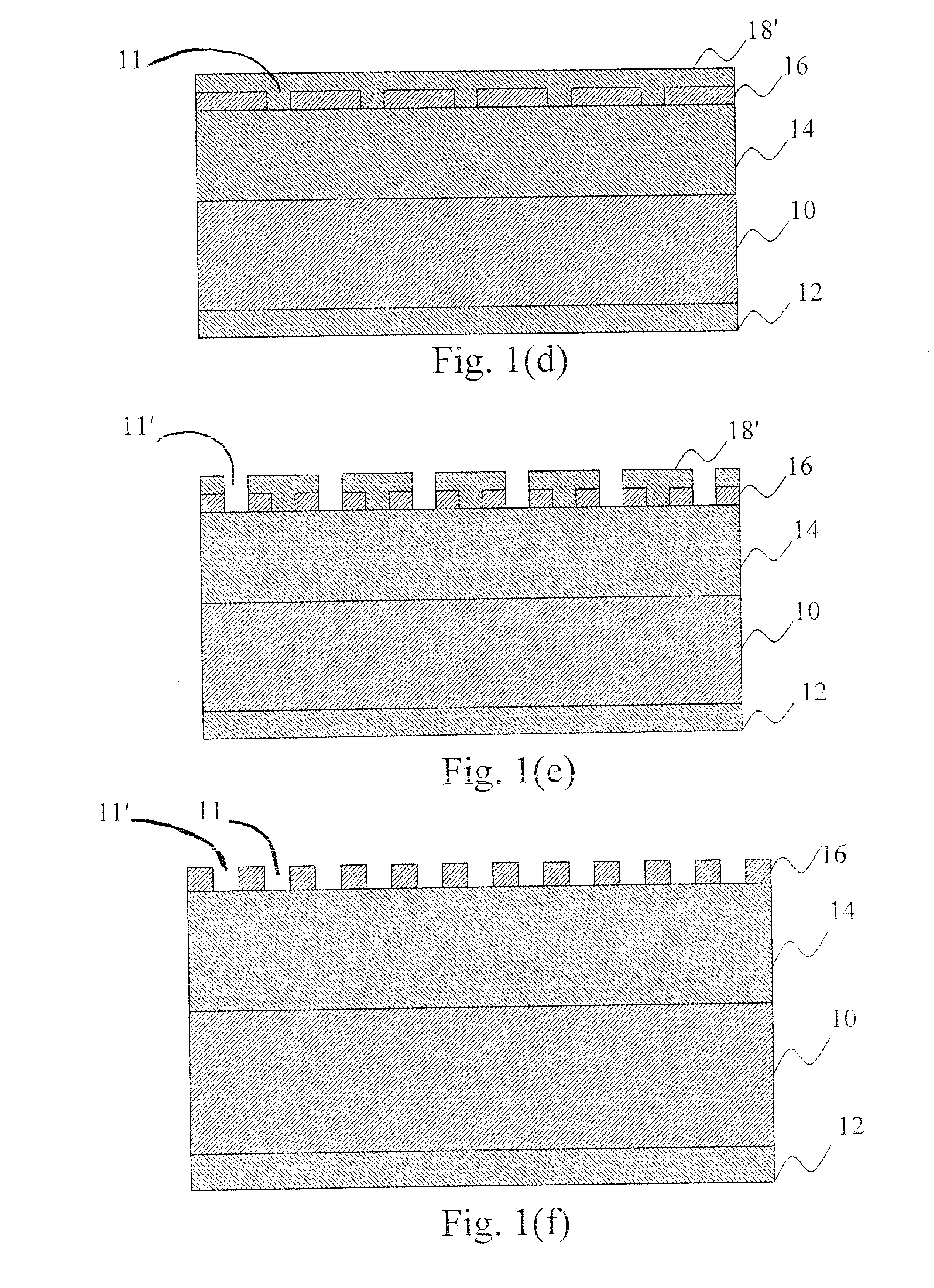
[0048]In this Example, a film stack was prepared using hardmask formulation I from Example 1. The developer-soluble hardmask was spin-coated onto a silicon substrate (100-mm wafer) at 2,000 rpm for 40 seconds, followed by a two-step thermal curing process. In particular, the wafer was heated at 120° C. for 40 seconds and then at 200° C. for 60 seconds on a hotplate. The thermally-set, developer-soluble hardmask formed a film having a thickness of 75 nm.

[0049]A commercial photoresist for i-line (365-nm) photolithography (SPR-950, from Rohm and Haas) was diluted with 2-heptanone to one-fifth of the original solids content. The diluted photoresist was spin-applied onto the hardmask to form an imaging layer. The wafer was then baked at 90° C. for 60 seconds as a post-application bake (“PAB”). The imaging layer had a thickness of 80 nm.

[0050]Next, the wafer was exposed with a photomask on a GCA Model 3300™ stepper NA=0.43) to radia...

example 3

Synthesis of Silicon-Containing Polymer for Hardmask Formulation II

[0052]In this procedure, 2 grams of styrene (Aldrich, Milwaukee, Wis.), 5.6 grams of methacrylic acid (Aldrich, Milwaukee, Wis.), and 12.4 grams of methacryloxymethyltrimethylsilane (Gelest, Morrisville, Pa.) were dissolved in 180 grams of PGME in a 3-neck round-bottom flask. The flask was degassed with dry nitrogen for 10-20 minutes. Next, 1 gram of azobisisobutyronitrile (AIBN, Aldrich, Milwaukee, Wis.) as a catalyst was added, and the mixture was stirred at room temperature until the catalyst completely dissolved. The flask with was then immersed into a preheated oil bath of 80° C. Nitrogen was introduced to the flask at a rate of about 5 mL / min. A condenser with water cooling was fitted into the center neck of the flask for refluxing. After 16 hours of reaction under constant stirring, the flask was removed from the oil bath and cooled down in the air to room temperature.

[0053]The contents of the flask were then ...


PUM

PropertyMeasurementUnit
thicknessaaaaaaaaaa
wavelengthsaaaaaaaaaa

Abstract

This invention provides methods of creating via or trench structures on a developer-soluble hardmask layer using a multiple exposure-development process. The hardmask layer is patterned while the imaging layer is developed. After the imaging layer is stripped using organic solvents, the same hardmask can be further patterned using subsequent exposure-development processes. Eventually, the pattern can be transferred to the substrate using an etching process.

Description

RELATED APPLICATIONS[0001]This application claims the priority benefit of a provisional application entitled ON-TRACK PROCESS FOR PATTERNING HARDMASK BY MULTIPLE DARK FIELD EXPOSURES, Ser. No. 61 / 024,474, filed Jan. 29, 2008, incorporated by reference herein.BACKGROUND OF THE INVENTION[0002]1. Field of the Invention[0003]The present invention relates in general to the process of fabricating semiconductor structures by microphotolithography and, more particularly, by multiple exposures for pitch multiplication.[0004]2. Description of the Prior Art[0005]The advances of microelectronic manufacture are reflected by the density and dimensions of semiconductor structures created by the microphotolithographic process. The demand for high density and small critical dimension (CD) has been constantly pushing photolithography technology to its limits. At the limits of a photolithographic process, features with relaxed pitch can be created with a smaller CD than that with high pitches, e.g., 1...

Claims


Application Information

Patent Timeline
Patent Type & Authority Applications(United States)
IPC IPC(8): G03F1/00G03F7/20
CPCG03F7/0752G03F7/11H01L21/0271H01L21/312H01L21/0337H01L21/0338H01L21/0332G03F7/0035G03F7/0758G03F7/095G03F7/322H01L21/02118H01L21/0274
Inventor SUN, SAM X.XU, HAOFLAIM, TONY D.
Owner BREWER SCI
Why Eureka
Try Eureka