Method for manufacturing soi substrate

a manufacturing method and semiconductor technology, applied in the direction of semiconductor devices, basic electric elements, electrical equipment, etc., can solve the problems of increasing bonding defects, increasing bonding defects, and generating large number of voids, so as to achieve sufficient bonding strength, reduce bonding defects, and improve adhesiveness between a single crystal semiconductor layer and a semiconductor substrate.

Inactive Publication Date: 2009-08-06
SEMICON ENERGY LAB CO LTD
View PDF20 Cites 16 Cited by
  • Summary
  • Abstract
  • Description
  • Claims
  • Application Information

AI Technical Summary

Benefits of technology

[0013]In view of the above problems, an object of the present invention is to improve adhesiveness between a single crystal semiconductor layer and a semiconductor substrate, and to reduce bonding defects. Further, another object is to provide a method for manufacturing an SOI substrate having sufficient bonding strength in a bonding step and also in a process of manufacturing a semiconductor device.
[0027]According to the present invention disclosed herein, an SOI substrate can be manufactured in which adhesiveness between a single crystal semiconductor layer and a semiconductor substrate is improved; bonding defects are reduced; and sufficient bonding strength is provided in a bonding step and also in a process of manufacturing a semiconductor device.

Problems solved by technology

In a process of bonding two single crystal silicon substrates, however, if minute foreign matters (e.g., particles) attach to a bonding interface between the single crystal silicon substrates, a large number of voids are generated, which increases bonding defects.
Further, if water molecules at the bonding interface between the single crystal silicon substrates are not diffused or absorbed into surroundings, water accumulates at the bonding interface, which increases bonding defects.
Furthermore, a dehydration condensation reaction does not proceed at the bonding interface, so that a strong bond is not formed and there occurs a bonding defect.
If there frequently occur such bonding defects, the bonding strength decreases and a thin single crystal silicon layer can come to be unstuck at the bonding interface between the single crystal silicon substrate which functions as the base substrate and the thin single crystal silicon layer which has been separated.
Further, also in manufacturing a semiconductor device, such bonding defects hinder manufacture of a semiconductor device having high quality.

Method used


Image

  • Method for manufacturing soi substrate
  • Method for manufacturing soi substrate
  • Method for manufacturing soi substrate

Examples


embodiment mode 1

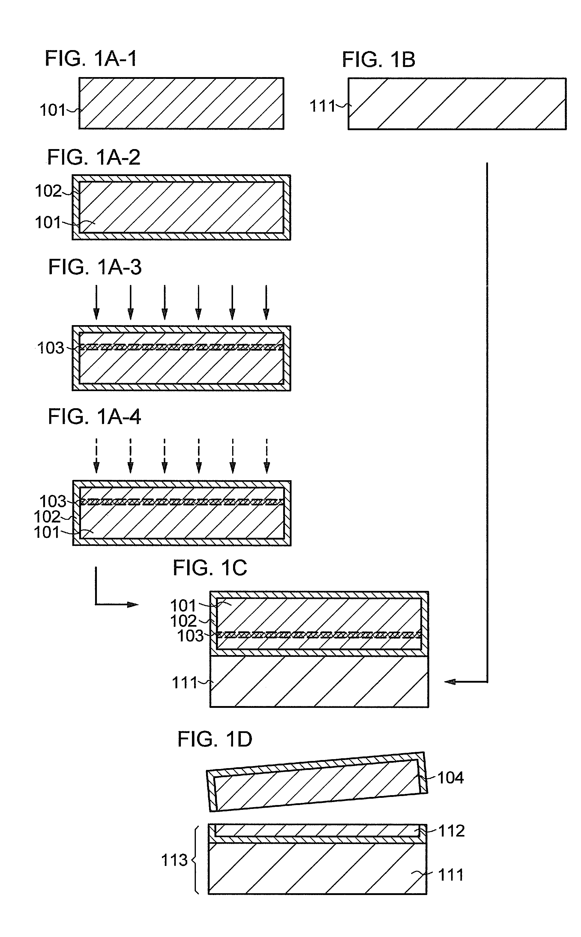
[0047]This embodiment mode describes an example of a method for manufacturing an SOI substrate with reference to the drawings. Specifically, a method is described in which a Si-based insulating film is formed on a single crystal semiconductor substrate side; the insulating film undergoes an O2 plasma treatment; then, the single crystal semiconductor substrate and a semiconductor substrate are bonded to each other.

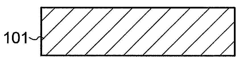
[0048]First, a single crystal semiconductor substrate 101 is prepared, and is cleaned with a sulfuric acid / hydrogen peroxide mixture (SPM), an ammonia / hydrogen peroxide mixture (APM), a hydrochloric acid / hydrogen peroxide mixture (HPM), dilute hydrofluoric acid (DHF), ozone water, or the like as appropriate (see FIG. 1A-1). For the single crystal semiconductor substrate 101, a commercial single crystal semiconductor substrate can be used; for example, a single crystal silicon substrate, a single crystal germanium substrate, or a compound semiconductor substrate such as a ga...

embodiment mode 2

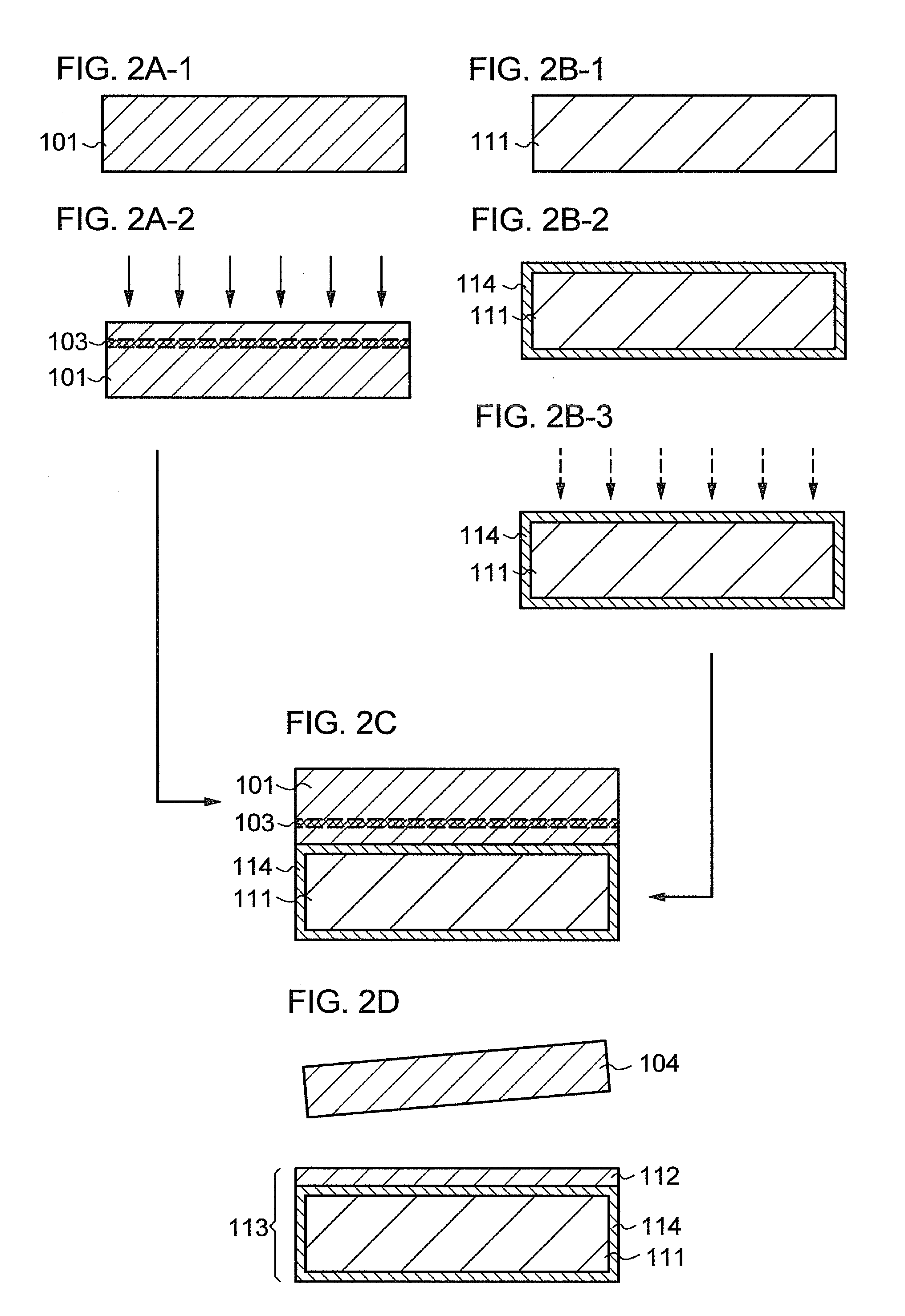
[0093]This embodiment mode describes a method for manufacturing an SOI substrate which is different from that of the preceding embodiment mode with reference to the drawings. Specifically, a method is described in which after forming a Si-based insulating film on a semiconductor substrate side and treating the insulating film with oxygen plasma, the semiconductor substrate and a single crystal semiconductor substrate in which an embrittlement layer is formed are bonded to each other. Hereinafter, the same reference numerals are given to parts with similar structures to those of Embodiment Mode 1, and description thereof is omitted.

[0094]First, a single crystal semiconductor substrate 101 is prepared, and is cleaned with a sulfuric acid / hydrogen peroxide mixture (SPM), an ammonia / hydrogen peroxide mixture (APM), a hydrochloric acid / hydrogen peroxide mixture (HPM), dilute hydrofluoric acid (DHF), ozone water, or the like as appropriate (see FIG. 2A-1).

[0095]Next, a protective layer (n...

embodiment mode 3

[0118]This embodiment mode describes a method for manufacturing an SOI substrate which is different from those presented in the preceding embodiment modes with reference to the drawings. Specifically, a method is described in which after forming an insulating film on each of a single crystal semiconductor substrate and a semiconductor substrate and treating the insulating film formed on the single crystal semiconductor substrate with plasma, the semiconductor substrate and the single crystal semiconductor substrate are bonded to each other. Hereinafter, the same reference numerals are given to parts with similar structures to those of Embodiment Modes 1 and 2, and description thereof is omitted.

[0119]First, a single crystal semiconductor substrate 101 is prepared in which an insulating film 102 has been formed on a surface; an embrittlement layer 103 has been formed in a region at a predetermined depth from a surface; and the insulating film 102 has undergone a plasma treatment by a...


PUM

PropertyMeasurementUnit
diametersaaaaaaaaaa
diametersaaaaaaaaaa
diametersaaaaaaaaaa

Abstract

A method for manufacturing an SOI substrate is provided in which adhesiveness between a single crystal semiconductor substrate and a semiconductor substrate is improved; bonding defects are reduced; and sufficient bonding strength is provided in a bonding step and also in a process of manufacturing a semiconductor device. An insulating film including halogen is formed on a single crystal semiconductor substrate side in which an embrittlement layer is formed. The insulating film including halogen undergoes a plasma treatment. The insulating film including halogen and a face of a semiconductor substrate are bonded so as to face each other. A thermal treatment is performed to split the single crystal semiconductor substrate along the embrittlement layer, thereby separating the single crystal semiconductor substrate into a single crystal semiconductor substrate and the semiconductor substrate to which a single crystal semiconductor layer is bonded. The single crystal semiconductor layer bonded to the semiconductor substrate undergoes a planarization treatment.

Description

BACKGROUND OF THE INVENTION[0001]1. Field of the Invention[0002]The present invention relates to a semiconductor device having a semiconductor layer formed over an insulating layer, and to a method for manufacturing the semiconductor device.[0003]2. Description of the Related Art[0004]In recent years, an integrated circuit has been developed in which an SOI (silicon on insulator) substrate is used instead of a bulk silicon wafer. By taking advantage of properties of a thin single crystal silicon layer formed over an insulating layer, a semiconductor layer in transistors in an integrated circuit can be separated completely, and the transistors can be a complete depletion type; thus, a semiconductor integrated circuit with high added value such as high integration, high-speed driving, or low power consumption can be realized.[0005]As an SOI substrate, a SIMOX substrate and a bonding substrate are known. For example, in a SIMOX substrate, an SOI structure is achieved by implanting oxyg...

Claims


Application Information

Patent Timeline
Patent Type & Authority Applications(United States)
IPC IPC(8): H01L21/762
CPCH01L21/76254H01L29/66772H01L27/1266H01L27/1214H01L21/20
Inventor OHNUMA, HIDETOYAMAZAKI, SHUNPEI
Owner SEMICON ENERGY LAB CO LTD
Why Eureka
Try Eureka