Single-polycrystalline silicon electrically erasable and programmable nonvolatile memory device

a nonvolatile memory, single-polycrystalline silicon technology, applied in the direction of digital storage, solid-state devices, instruments, etc., can solve the problems of high voltage breakdown of peripheral devices of nvm arrays, incompatible high-voltage breakdown voltages with current process technology, and high voltage breakdown voltages

Inactive Publication Date: 2009-08-13
APLUS FLASH TECH
View PDF21 Cites 54 Cited by
  • Summary
  • Abstract
  • Description
  • Claims
  • Application Information

AI Technical Summary

Benefits of technology

[0013]An object of this invention is to provide a single-polycrystalline floating gate NVM memory cell that is very compatible with the existing single polycry

Problems solved by technology

The required voltages for performing a program and erase operation are too high for devices that are fabricated using standard CMOS logic process.
The peripheral devices of the NVM array thus require a high voltage breakdown for the operation.
The high-voltage breakdown voltages are not compatible with the current process technology for the peripheral single-poly

Method used


Image

  • Single-polycrystalline silicon electrically erasable and programmable nonvolatile memory device
  • Single-polycrystalline silicon electrically erasable and programmable nonvolatile memory device
  • Single-polycrystalline silicon electrically erasable and programmable nonvolatile memory device

Examples


Embodiment Construction

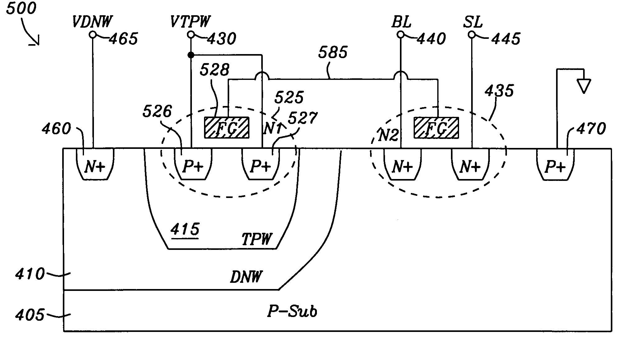
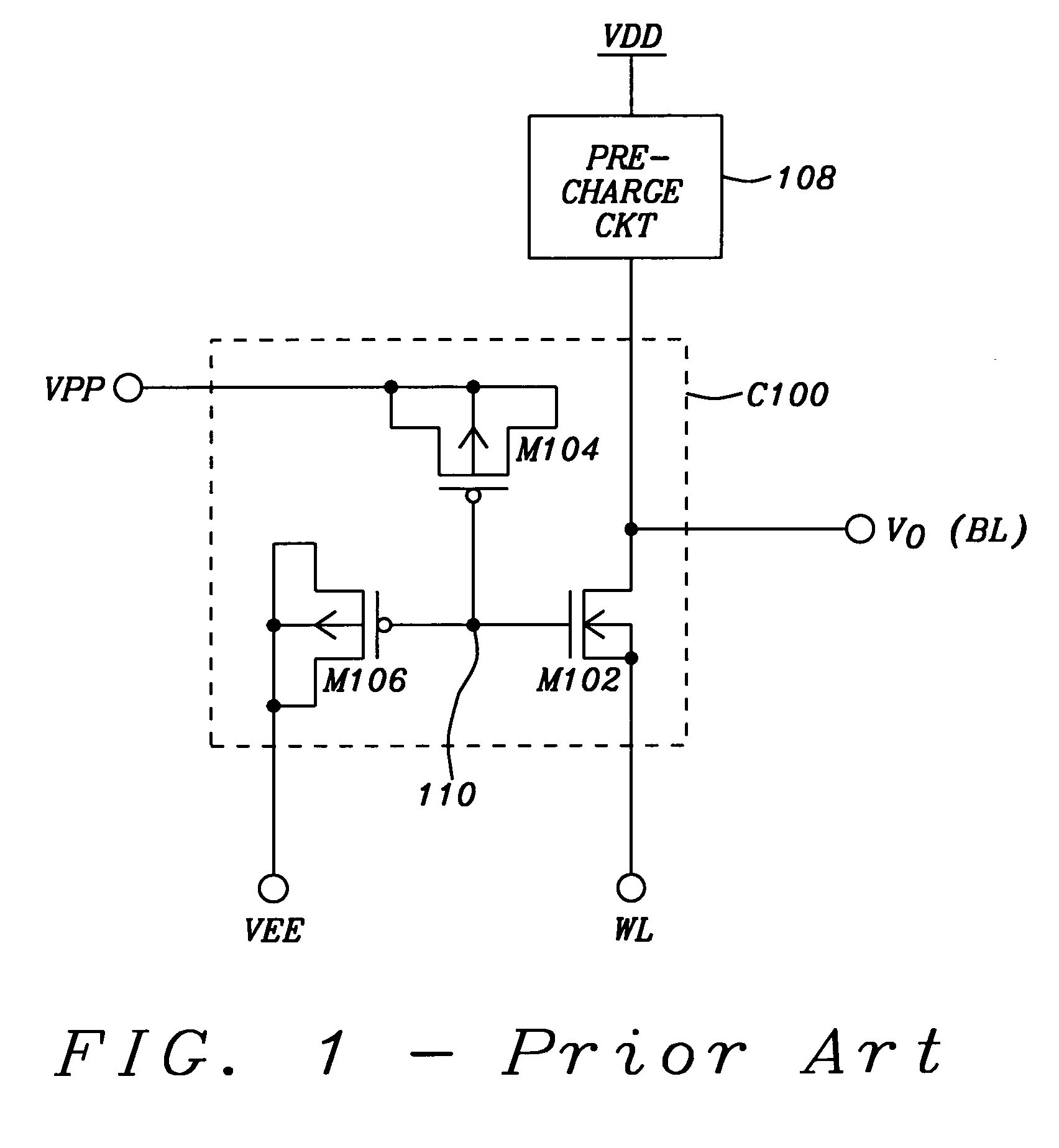
[0075]Refer now to FIG. 1 for a description of the schematic diagram of a single polycrystalline silicon floating gate nonvolatile memory cell of Wang et al. Wang et al. provides a single-polycrystalline floating gate one transistor flash cell structure. The NVM cell C100 includes a first programming transistor M106, second programming transistor M104, and storage transistor M102. The pre-charge circuit 108 pre-charges the storage transistor M102 at the beginning of the read operation with a high power supply voltage source VDD. The first programming transistor M106 and the second programming transistor M104 together form the programming element of cell C100. The First programming transistor M106 and the second programming transistor M104 have their gates coupled together and share the floating node 110 with storage transistor M102. A source, a drain, and an n-well terminal of the first programming transistor M106 are coupled together to a first programming voltage VEE. A source, a ...


PUM


Abstract

A single polycrystalline silicon floating gate nonvolatile memory cell has a MOS capacitor and a storage MOS transistor fabricated with dimensions that allow fabrication using current low voltage logic integrated circuit process. The MOS capacitor has a first plate connected to a gate of the storage MOS transistor to form a floating gate node. The physical size of the MOS capacitor is relatively large (approximately 10 time greater) when compared to a physical size of the storage MOS transistor to establish a large coupling ratio (approximately 90% between the second plate of the MOS capacitor and the floating gate node. When a voltage is applied to the second plate of the MOS capacitor and a voltage applied to the source region or drain region of the MOS transistor establishes a voltage field within the gate oxide of the MOS transistor such that Fowler-Nordheim edge tunnel is initiated.

Description

[0001]This application claims priority under 35 U.S.C. §119 to U.S. Provisional Patent Application Ser. No. 61 / 065,418, filed on Feb. 11, 2008, which is herein incorporated by reference in its entirety.BACKGROUND OF THE INVENTION[0002]1. Field of the Invention[0003]This invention relates generally to a non-volatile integrated circuit memory. More particularly this invention relates to single polycrystalline silicon floating gate electrically erasable programmable read only memory (EEPROM) and flash electrically erasable programmable read only memory (flash memory).[0004]2. Description of Related Art[0005]In the semiconductor industry, generally, there are two important kinds of CMOS memories—“volatile” and “non-volatile”. The “volatile” memory, in which the stored data is not retained when its low-voltage VDD power supply is removed or shut down. The volatile memories include Static Random Access Memory (SRAM) and Dynamic Random Access Memory (DRAM).[0006]The “non-volatile” memory (...

Claims


Application Information

Patent Timeline
IPC IPC(8): G11C16/06H01L29/788H01L29/94
CPCG11C16/0441G11C2216/10H01L29/7883H01L29/42324H01L27/11558H10B41/60
Inventor LEE, PETER WUNGHSU, FU-CHANG
Owner APLUS FLASH TECH
Why Eureka
Try Eureka