Method for manufacturing photoelectric conversion device

a technology of photoelectric conversion and manufacturing method, which is applied in the direction of semiconductor/solid-state device manufacturing, semiconductor devices, electrical apparatus, etc., can solve the problems of increased manufacturing cost, difficult to obtain favorable uneven structure only by etching, and easy varying size of formed uneven structure, etc., to reduce the reflection of incident light, improve absorption, and reduce the effect of consumption of silicon as a material

Inactive Publication Date: 2009-08-20
SEMICON ENERGY LAB CO LTD
View PDF28 Cites 27 Cited by
  • Summary
  • Abstract
  • Description
  • Claims
  • Application Information

AI Technical Summary

Benefits of technology

[0012]In the conventional method for etching with use of an alkaline solution or the like, unevenness formed by dipping in an alkaline solution using different etching rates depending on a crystal plane orientation to form unevenness; however, the size of the formed uneven structure varies easily due to a change in the concentration of the alkaline solution in the dipping, for example. In the case of polycrystalline silicon, its crystal plane orientation is more random than that of the single crystal silicon. Therefore, the favorable uneven structure is hard to be obtained only by etching. As described above, although the uneven structure can be formed by using the combination of the laser-processing technique and the etching, the step is additionally required if using the combination, whereby a manufacturing cost is increased. Further, silicon is evaporated by irradiation with a laser beam to form grooves, whereby particles are easily generated, and further, there is possibility of reattachment of the evaporated silicon as a particle.
[0013]In view of the aforementioned problems, one object of the present invention is to provide a method for manufacturing a photoelectric conversion device with excellent photoelectric conversion characteristics typified by a solar cell, using a silicon material effectively, and provide the photoelectric conversion device manufactured by the method.
[0026]According to the present invention, the surface uneven structure can be formed on the light incident side of the photoelectric conversion device, which can reduce reflection of incident light and improve absorptance with respect to light. The single crystal silicon layer or the polycrystalline silicon layer obtained by slicing a superficial portion of the single crystal silicon substrate or the polycrystalline silicon substrate is bonded to the supporting substrate, whereby consumption of silicon as a material can be suppressed. The single crystal silicon substrate from which the first single crystal silicon layer has been separated and the polycrystalline silicon substrate from which the polycrystalline silicon layer has been separated can be reused. Accordingly, the photoelectric conversion device with excellent photoelectric conversion characteristics can be provided while using resources efficiently.

Problems solved by technology

However, although photoelectric conversion efficiency is improved by forming the surface textual structure by etching, a silicon material is to be removed, which is to waste of the silicon material.
In the conventional method for etching with use of an alkaline solution or the like, unevenness formed by dipping in an alkaline solution using different etching rates depending on a crystal plane orientation to form unevenness; however, the size of the formed uneven structure varies easily due to a change in the concentration of the alkaline solution in the dipping, for example.
Therefore, the favorable uneven structure is hard to be obtained only by etching.
As described above, although the uneven structure can be formed by using the combination of the laser-processing technique and the etching, the step is additionally required if using the combination, whereby a manufacturing cost is increased.

Method used


Image

  • Method for manufacturing photoelectric conversion device
  • Method for manufacturing photoelectric conversion device
  • Method for manufacturing photoelectric conversion device

Examples


embodiment mode 1

[0056]One aspect of the present invention is that silicon for photoelectric conversion is irradiated with a laser beam through an optical modulator, which modulates light intensity of a laser bean regularly, whereby a silicon layer with an uneven structure is formed. Description is hereinafter made with reference to drawings.

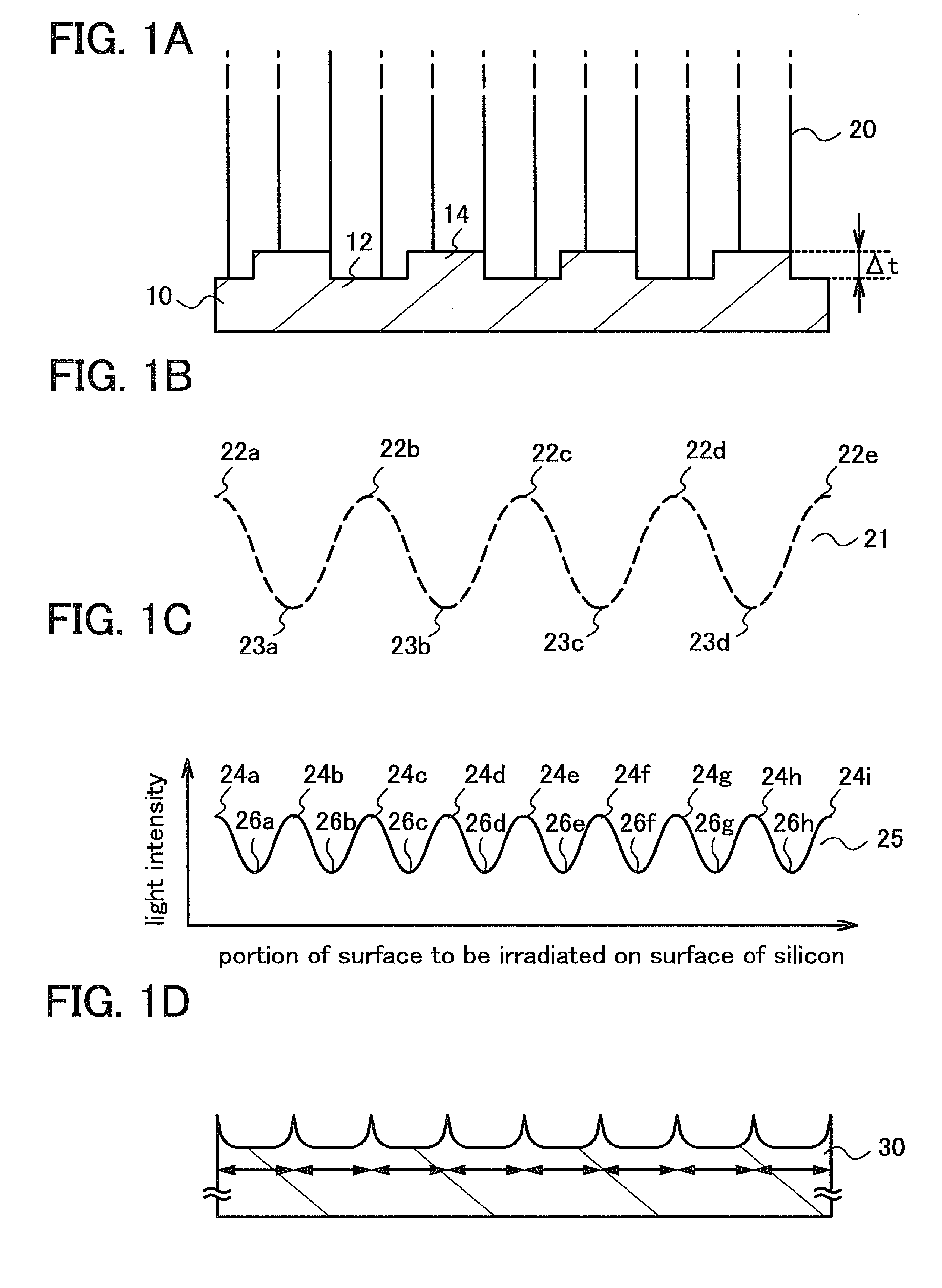
[0057]FIGS. 1A to 1D are schematic views for explaining formation of unevenness in a silicon 30 by irradiation with a laser beam 20 through a phase shift mask 10 that is one mode of an optical modulator.

[0058]In FIG. 1A, the optical modulator modulates light intensity of the laser beam regularly. Described in this embodiment mode is an example in which a phase of the laser beam is modulated regularly using a phase shift mask 10 as the optical modulator, a light intensity distribution in which a light intensity is modulated regularly is obtained. Here, the phase shift mask refers to a mask which shifts a phase of transmitted light of an adjacent pattern by π. The...

embodiment mode 2

[0076]In this embodiment mode, a method for manufacturing a photoelectric conversion device in which unevenness is formed in a silicon layer for photoelectric conversion by irradiation with a laser beam using an optical modulator and a structure of the photoelectric conversion device formed by the method will be described.

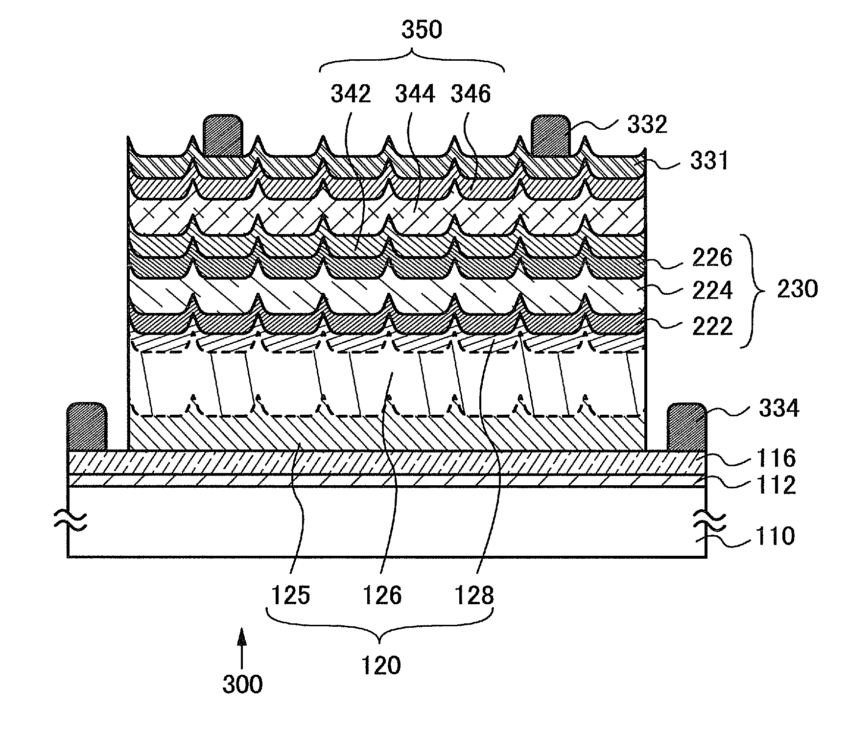
[0077]FIG. 3A illustrates an example of a top view of a photoelectric conversion device 100 according to this embodiment mode and FIG. 3B illustrates an example of a cross sectional view thereof. Note that FIG. 3B is the example of the cross sectional view taken along the line OP in FIG. 3A.

[0078]In the photoelectric conversion device 100, a first unit cell 120 in which a single crystal silicon layer is provided is formed over a supporting substrate 110. The first unit cell 120 is provided with the first electrode 116 on the supporting substrate 110 side, and the first unit cell 120 is provided with a second electrode 132 on a surface side which is opposite to the ...

embodiment mode 3

[0173]In this embodiment mode, an example of a method for manufacturing a photoelectric conversion device which is different from that in the aforementioned embodiment mode will be described. Described in the aforementioned embodiment mode is the example in which laser treatment is performed on the first single crystal silicon layer 124 which has been separated from the single crystal silicon substrate 101, using the optical modulator to form the uneven structure on a surface. In this embodiment mode, a method for forming unevenness on a second single crystal silicon layer, which is obtained by epitaxial growth of the single crystal silicon layer separated from the single crystal silicon substrate 110, by performing laser treatment using an optical modulator will be described. Note that other structures are based on the aforementioned embodiment mode and description thereof is omitted.

[0174]The aforementioned steps up to FIG. 5B are performed and the impurity silicon layer 122 and t...


PUM


Abstract

The purpose is manufacturing a photoelectric conversion device with excellent photoelectric conversion characteristics typified by a solar cell with effective use of a silicon material. A single crystal silicon layer is irradiated with a laser beam through an optical modulator to form an uneven structure on a surface thereof. The single crystal silicon layer is obtained in the following manner; an embrittlement layer is formed in a single crystal silicon substrate; one surface of a supporting substrate and one surface of an insulating layer formed over the single crystal silicon substrate are disposed to be in contact and bonded; heat treatment is performed; and the single crystal silicon layer is formed over the supporting substrate by separating part of the single crystal silicon substrate fixed to the supporting substrate along the embrittlement layer or a periphery of the embrittlement layer. Then, irradiation with a laser beam is performed on a separation surface of the single crystal silicon layer through an optical modulator which modulates light intensity regularly, and unevenness is formed on the surface. Due to the unevenness, reflection of incident light is reduced and absorptance with respect to light is improved, therefore, photoelectric conversion efficiency of the photoelectric conversion device is improved.

Description

BACKGROUND OF THE INVENTION[0001]1. Field of the Invention[0002]The present invention relates to a photoelectric conversion device including single crystal silicon or polycrystalline silicon and to a manufacturing method thereof.[0003]2. Description of the Related Art[0004]Since the situation of global warming has been serious, a measure against the global warming is an issue that needs to be addressed worldwide. Most greenhouse effect gases which are regarded as a main cause for global-warming, such as carbon dioxide, are exhausted by consumption of energy, such as oil, coals, and natural gases. However, such energy is indispensable to the industrial society. Therefore, the amount of energy consumption cannot be reduced simply. Thus photoelectric power generation which discharges less amount of carbon dioxide and which is eco-friendly has attracted attentions as the next-generation energy.[0005]For the photoelectric power generation, a silicon photoelectric conversion device, which...

Claims


Application Information

Patent Timeline
Patent Type & Authority Applications(United States)
IPC IPC(8): H01L31/0216
CPCH01L31/022425H01L31/0236H01L31/03685H01L31/03762Y02E10/547H01L31/1892Y02E10/548Y02E10/545H01L31/068H01L31/02363
Inventor ISAKA, FUMITOKATO, SHOMOMO, JUNPEI
Owner SEMICON ENERGY LAB CO LTD
Why Eureka
Try Eureka