
Resonant cavity color conversion el device and organic el display device using the same

a color conversion and display device technology, applied in the direction of discharge tube/lamp details, discharge tube/solid-state device testing/measurement, discharge tube/lamp details, etc., can solve the problems of complex manufacturing process, light emission efficiency, and difficulty in making up a complete display device, and achieve high luminance color, simple manufacturing method, and high efficiency

Active Publication Date: 2009-08-27
GLOBAL OLED TECH
View PDF4 Cites 44 Cited by
  • Summary
  • Abstract
  • Description
  • Claims
  • Application Information

AI Technical Summary

Benefits of technology

[0013]The present invention has been made to solve these difficulties that arise in practical application of the resonant cavity EL element and the fluorescence conversion method to a color display device, and provides a high luminance color display device implementing high efficiency EL elements employing a simple manufacturing method.
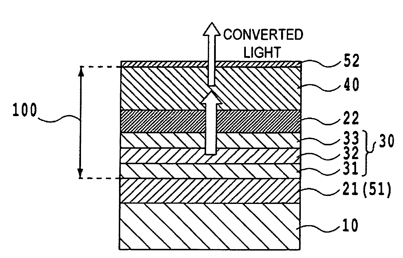
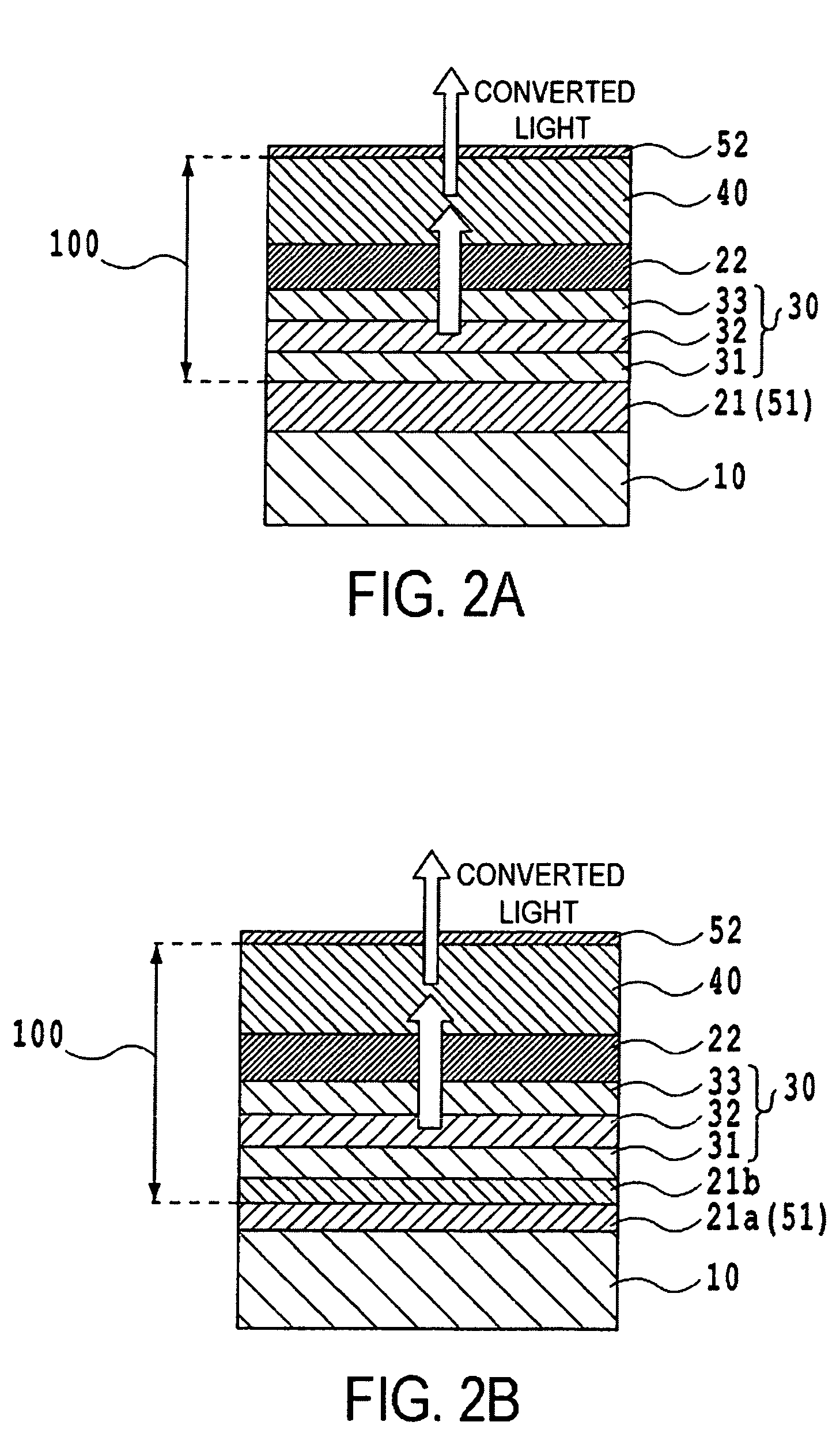
[0023]In the resonant cavity color conversion organic EL element having a structure described above, the color conversion layer is disposed between a pair of reflective layers that compose a microcavity structure and the optical path length of the microcavity structure is adjusted to fit to the resonance condition of the light with a specific wavelength emitted from the color conversion layer, thereby intensifying the converted light from the color conversion layer. When the color conversion layer is formed of solely one or more types of organic dyes, in particular, the refractive index of the color conversion layer can be made nearly equal to the refractive index of the thin film materials composing the EL element. As a result, the color conversion layer absorbs most of the light emitted by the light-emitting layer and performs fluorescent conversion, further intensifying the converted light from the color conversion layer.

Problems solved by technology

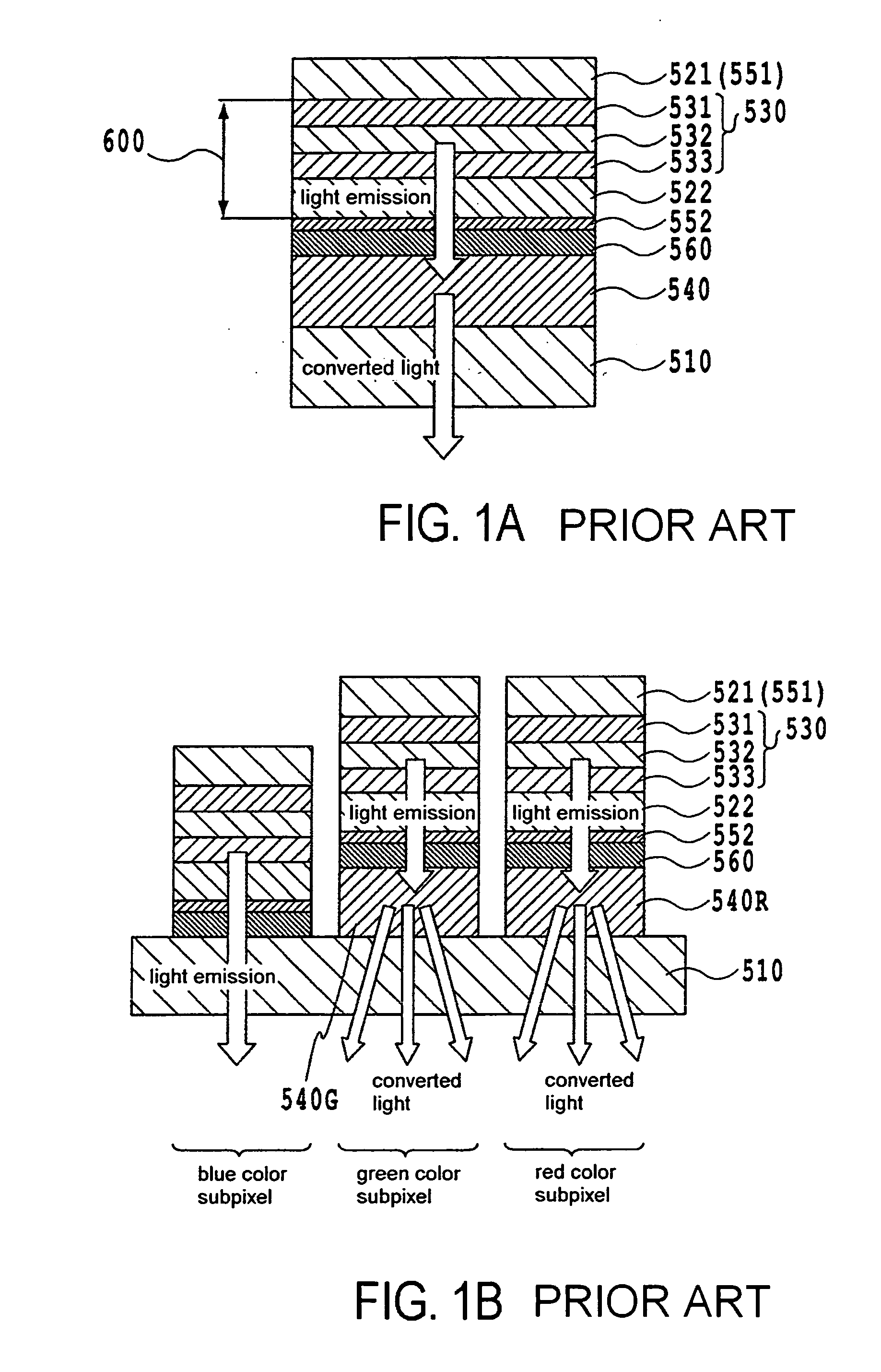
It is well known that one of the reasons for the limitation of the light emission efficiency of an EL element is the fact that more than half of light generated in the light-emitting layer is confined within the element or a transparent substrate, see, for example, Non-patent Document 1, i.e., Advanced Materials, Vol. 6, p.
Thus, the manufacturing process is complicated.
Therefore, there are difficulties connected with making up a complete display device.
Therefore, the device of FIG. 1(b) is not well suited for practical application.

Method used


Image

  • Resonant cavity color conversion el device and organic el display device using the same
  • Resonant cavity color conversion el device and organic el display device using the same
  • Resonant cavity color conversion el device and organic el display device using the same

Examples


example 1

Resonant Cavity Color Conversion EL Element Emitting Red Color Light

[0095]A substrate of Corning 1737 glass having dimensions of a length of 50 mm, a width of 50 mm, and a thickness of 0.7 mm was prepared, cleaned with alkali detergent, and rinsed thoroughly with deionized water. On the cleaned substrate, a silver alloy (APC-TR, a product of Furuya Metal Co., Ltd.) was deposited to form a 100 nm-thick silver alloy film by a DC magnetron sputtering method. On the silver alloy film, a film of photoresist (TFR-1250, a product of Tokyo Ohka Kogyo Co., Ltd.) having a thickness of 1.3 μm was spin-coated and dried in a clean oven at 80° C. for 15 min. On the photoresist film, ultraviolet light was irradiated by a high-pressure mercury vapor lamp through a photomask having a stripe pattern with a width of 2 mm. Being developed with a developer (NMD-3, a product of Tokyo Ohka Kogyo Co., Ltd.), a photoresist pattern with a width of 2 mm was created on the silver alloy thin film. After etching...

example 2

Resonant Cavity Color Conversion EL Element for Red Color Light Emission

[0101]A resonant cavity color conversion EL element for red color light emission was obtained in the same procedure as in Example 1 except that the thickness of the color conversion layer was changed to 330 nm and the thickness of the semi-transparent reflective layer was changed to 20 nm.

example 3

Resonant Cavity Color Conversion EL Element for Green Color Light Emission

[0104]A resonant cavity color conversion EL element for green color light emission was obtained in the same procedure as in Example 1 except that a color conversion layer was formed by depositing solely Alq3 and the thickness of the color conversion layer was changed to 230 nm. FIG. 7 shows an emission spectrum of the obtained element. Table 2 shows evaluation results on chromaticity and electric current efficiency (at a current density of 10 mA / cm2). The results of FIG. 7 and Table 2 have demonstrated that introduction of a microcavity structure in the invention gives green color light with excellent color purity even by using Alq3, which exhibits a broad emission spectrum as for a green color conversion dye. The interface that exhibited largest difference in refractive index within the microcavity structure in this Example 3 was also the interface between the electron injection layer (lithium-doped Alq3, ref...


PUM


Abstract

A resonant cavity color conversion EL element in which intensity of converted light from a color conversion layer is increased and an organic EL display device in which viewing angle dependence of the color tone is small and the manufacturing process is simple. The EL element includes at least a pair of electrodes; a functional layer includes a light-emitting layer and is sandwiched by the pair of electrodes; a color conversion layer that absorbs light emitted from the light-emitting layer and emits light with a different wavelength; and a pair of light reflective layers. Notably, the pair of light reflective layers are composed of a non-transparent reflective layer and a semi-transparent reflective layer that have a distance therebetween that is set at an optical distance to construct a microcavity that increases intensity of light with a specific wavelength emitted from the color conversion layer.

Description

CROSS-REFERENCE TO RELATED APPLICATION[0001]This Application is based on, and claims priority to, Japanese Patent Application No. 2008-046862, filed on Feb. 27, 2008, the contents of which are incorporated herein by reference.BACKGROUND OF THE INVENTION[0002]1. Field of the Invention[0003]The present invention relates to a multicolor light-emitting electroluminescent device. A multicolor light-emitting electroluminescent device according to the invention can be used in appliances such as personal computers, word processors, TV sets, facsimiles, audio sets, video devices, car navigation devices, electronic calculators, telephones, portable terminals, and industrial instruments.[0004]2. Description of the Related Art[0005]With needs for diversity and space saving in information devices, extensive development efforts for flat panel displays that attain lower power consumption and smaller occupied space than CRTs have been in progress. In particular, expectations for electroluminescent ...

Claims


Application Information

Patent Timeline
Patent Type & Authority Applications(United States)
IPC IPC(8): H01J1/62
CPCH01L27/322H01L51/5265Y02E10/549H10K59/38H10K50/17H10K59/876H01L22/12H10K30/82H10K50/15H10K50/16H10K50/171H10K50/852
Inventor TERAO, YUTAKA
Owner GLOBAL OLED TECH
Learn More