Solid-state imaging device and method for producing the same

a solid-state imaging and imaging device technology, applied in semiconductor devices, radio-controlled devices, electrical devices, etc., can solve the problems of affecting the quality of solid-state imaging, and affecting the enhancement of overlap accuracy by photolithography, so as to reduce the distance, suppress the extension of the diffusion length of an impurity in the device region, and reduce the production cost

Inactive Publication Date: 2009-08-27
FUJIFILM CORP
View PDF12 Cites 1 Cited by
  • Summary
  • Abstract
  • Description
  • Claims
  • Application Information

AI Technical Summary

Benefits of technology

[0021]According to this constitution, the patterning of the light-shielding film is performed by the use of photolithography, so that the reliability can be more enhanced.(3) The method for producing the solid-state imaging device as described in the item (1) or (2), which comprises, etching at least a part of an gate oxide film on the photoelectric conversion section by using the charge transfer electrode as the mask, the etching performing in advance of the forming of the sidewall.
[0023]By virtue of this constitution, the antireflection film can be formed at a lower position and the intrusion of light can be more unfailingly prevented.(5) The method for producing the solid-state imaging device as described in the item (4), which comprises, covering the substrate surface with an oxide film by a radical oxidation using a low-temperature plasma after the exposing of the substrate surface.
[0030]By virtue of this constitution, dense and highly reliable insulation can be achieved.(12) The solid-state imaging device as described in the item (9), wherein a silicon oxide film formed by a radical oxidation using a low-temperature plasma is intervening between the antireflection film and the light-shielding film.(13) The solid-state imaging device as described in the item (9), wherein the antireflection film is a silicon nitride film.(14) The solid-state imaging device as described in the item (9), wherein the light-shielding film is tungsten.(15) The solid-state imaging device as described in the item (14), wherein the tungsten film is formed through a titanium nitride layer.
[0031]According to the present invention, high-level overlap accuracy is not necessary and in turn, an expensive exposure apparatus is not required, so that the production cost can be reduced.
[0032]Also, the island-like antireflection film shape intended to form on the photoelectric conversion section can be adjusted to the width of polysilicon sidewall, that is, the film thickness of deposit, so that self-aligning constitution can be established.
[0033]Furthermore, the insulating film and the like are formed by radical oxidation using a low-temperature plasma, so that extension of the diffusion length of an impurity in the device region can be suppressed and the light-shielding film can be reduced in the distance to the substrate by virtue of the descending of its bottom level, as a result, multiple reflection of obliquely incident light can be prevented.

Problems solved by technology

According to this structure, a light-shielding film 7 can be formed to unfailingly cover the charge transfer section, but since a silicon oxide film is formed below the light-shielding film so as to ensure electrical withstand voltage with the charge transfer electrode, there is a problem that multiple reflection is generated between the light-shielding film and the silicon substrate, and the obliquely incident light run into the charge transfer path worsens the smear.
Therefore, in increasing the number of pixels, it becomes an important problem to cover the charge transfer section with a light-shielding film and thoroughly open the opening of the photoelectric conversion section.
However, this method requires to take an alignment margin of the photolithography, and this stands as an obstacle hampering microfabrication.
That is, there is a problem that despite the need for extremely high-level overlap accuracy, enhancement of the overlap accuracy by photolithography is very difficult.
In this way, in the conventional solid-state imaging device shown in FIGS. 8A and 8E, displacement at the patterning of an antireflection film and a flattening film is a serious problem and sometimes causes fluctuation of sensitivity or worsening of smears.

Method used


Image

  • Solid-state imaging device and method for producing the same
  • Solid-state imaging device and method for producing the same
  • Solid-state imaging device and method for producing the same

Examples


embodiment 1

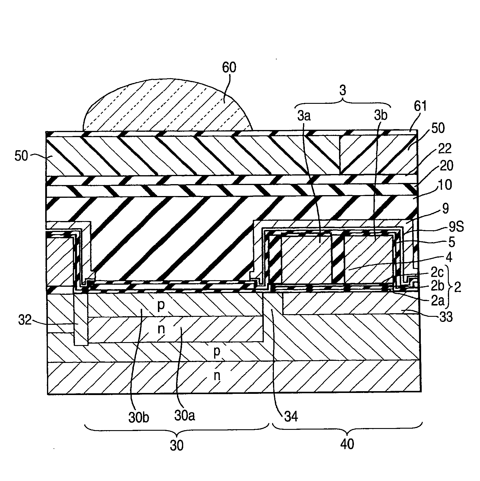
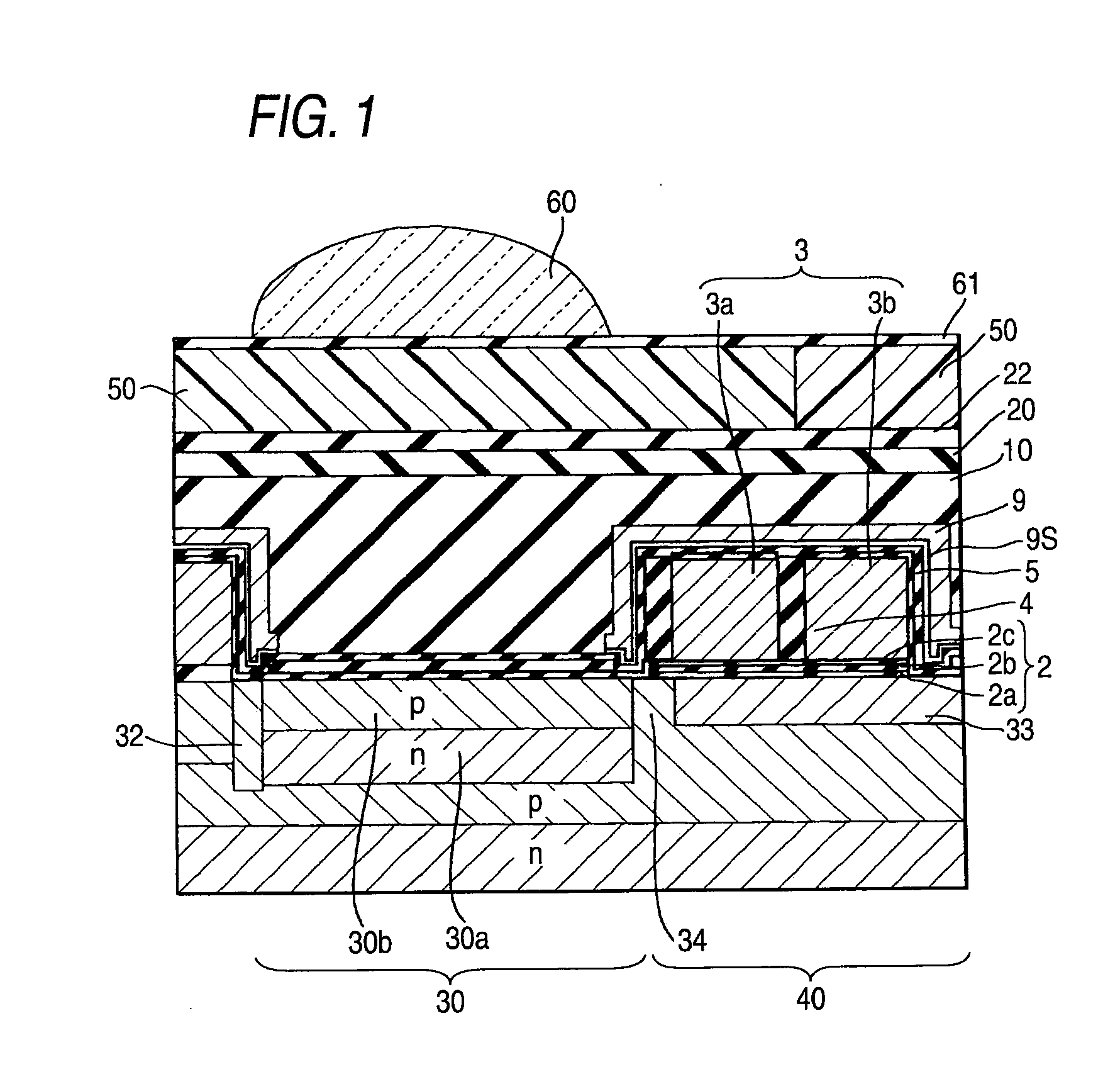
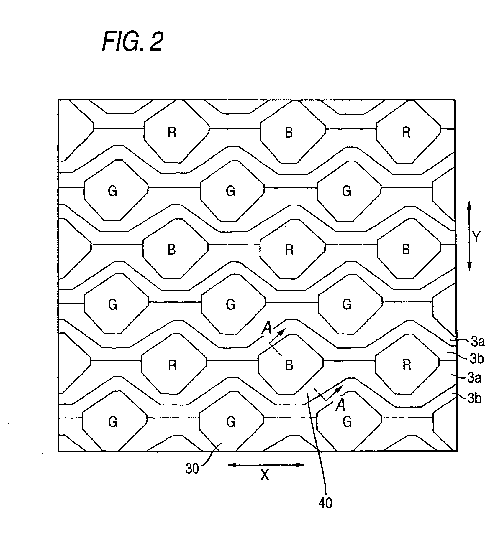
[0044]This solid-state imaging device has, as shown in FIGS. 1 and 2, a photoelectric conversion section, a charge transfer section equipped with a charge transfer electrode for transferring an electric charge generated in the photoelectric conversion section, and an antireflection film 7 formed in the photoelectric conversion section, wherein a light-shielding film covering the charge transfer electrode is formed to reach a level lower than the top surface of the antireflection film 7 and surround the periphery of the antireflection film. By virtue of this constitution, a high-precision high-sensitivity solid-state imaging device capable of blocking intrusion of light into the charge transfer section due to multiple reflection can be provided. Here, the antireflection film is composed of a silicon nitride film, and its top and bottom layers are covered with an insulating film comprising a silicon oxide film using a low-temperature plasma. FIG. 1 is a cross-sectional schematic view,...

embodiment 2

[0074]In Embodiment 1, on the photoelectric conversion section, the gate oxide film 2 is completely removed and a silicon oxide film 5 is formed by radical oxidation to cover the entire surface, but when the gate oxide film 2 is composed of an oxide nitride oxide (ONO) film, the antireflection film may be formed thereon.

embodiment 3

[0075]In Embodiment 1, the silicon oxide films 5 and 8 are formed by radical oxidation to sandwich the antireflection film and thereby cover the entire surface of the antireflection film, but if slight reduction in the passivation property is allowed, either one of those silicon oxide films may be omitted.

[0076]Also, the light-shielding metal is not limited to tungsten and may be appropriately changed to titanium (Ti), cobalt (Co), nickel (Ni) or the like.

[0077]Incidentally, the production method is not limited to the above-described Embodiments but may be appropriately changed.

[0078]As described in the foregoing pages, according to the present invention, an island-like antireflection film can be easily and self-alignedly formed on a photodiode with good controllability and this enables elevation of sensitivity and reduction of smears. Therefore, the present invention is effective for the fabrication of a fine and high-sensitivity solid-state imaging device such as compact camera. A...


PUM


Abstract

A method for producing a solid-state imaging device, which including: a photoelectric conversion section; a charge transfer section having a charge transfer electrode; and an antireflection film covering a light-receiving region in the photoelectric conversion section, wherein forming the antireflection film includes: forming a sidewall on a lateral wall of the charge transfer electrode after forming the charge transfer electrode; forming an antireflection film on a substrate surface where the sidewall is formed; forming a resist on the antireflection film; melting and flattening the resist to expose the antireflection film on the charge transfer electrode; removing the antireflection film by using the resist as the mask; removing the sidewall; covering the charge transfer electrode with an insulating film; and forming a light-shielding film that reaches a level lower than the top surface of the antireflection film, and that surrounds the periphery of the antireflection film.

Description

CROSS REFERENCE TO RELATED APPLICATIONS[0001]This application is a Divisional of co-pending application Ser. No. 11 / 517,487, filed on Sep. 8, 2006, the entire contents of which are hereby incorporated by reference and for which priority is claimed under 35 U.S.C. § 120.BACKGROUND OF THE INVENTION[0002]1. Field of the Invention[0003]The present invention relates to a solid-state imaging device and a production method thereof, more specifically, the present invention relates to a charge transfer electrode of a solid-state imaging device.[0004]2. Background Art[0005]The solid-state imaging device utilizing a charge coupled device (CCD) used for an area sensor and the like has a photoelectric conversion section comprising a photodiode or the like and a charge transfer section equipped with a charge transfer electrode for transferring a signal charge from the photoelectric conversion section. As for the charge transfer electrode, plural charge transfer electrodes are adjacently disposed ...

Claims


Application Information

Patent Timeline
Patent Type & Authority Applications(United States)
IPC IPC(8): H01L31/0232
CPCH01L27/1462H01L27/14685H01L27/14623
Inventor SATO, TAKANORI
Owner FUJIFILM CORP
Why Eureka
Try Eureka